In the process of integrated circuit chip operation, there will inevitably be power losses, and most of these power losses will be converted into heat energy and dissipated. Under abnormal conditions such as high environment and short circuit, the internal heat of the chip cannot be dissipated in time, which inevitably increases the working temperature of the chip. Excessively high operating temperature has a great influence on the chip's performance, reliability and safety. Studies have shown that for every 1 ° C increase in chip temperature, the drive capability of the MOS tube will decrease by about 4%, the connection delay will increase by 5%, and the integrated circuit failure rate will double. Therefore, there must be an over-temperature protection circuit inside the chip to protect Chip security.
This article will introduce an over-temperature protection circuit that can be implemented with a standard CMOS process. In circuit design, the current source proportional to temperature (PTAT current) and the junction voltage of PNP tube (parasitic in CMOS process) with negative temperature coefficient are used as two differential temperature sensing units. This differential sensing method can improve the sensitivity of the circuit to temperature changes. At the same time, it has a hysteresis function, which can effectively avoid damage to the chip due to thermal oscillation.
1 Architecture principle analysis
1.1 Analysis of working principle
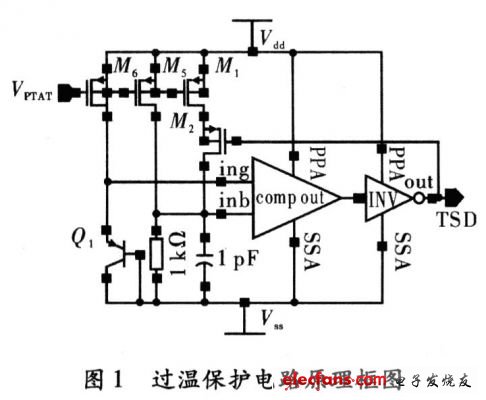
Figure 1 is the principle architecture of the design. Q1 is a parasitic PNP transistor in the NWELLCMOS process. Its collector must be connected to the location. In order to use the negative temperature characteristic of the parasitic PN junction to conduct the forward voltage, Q1 is connected as a diode The base set is also connected to ground), so that the voltage VA between point A and ground has the property that the forward voltage of the PN junction is inversely proportional to the temperature. Since the bias voltage output by the reference circuit is applied to the gates of M0, M1, and M5, PTAT current (ProporTIonal to Abso-lute Temperature) will be generated on its branch; while providing bias, it is also on the resistor R0 The voltage VB, which is proportional to the temperature, that is, the voltage at point B increases. When a certain temperature TH (set off temperature) is reached, VH≥VA, the comparator Comp outputs a high level, and after the inverter INV, the output TSD is a low level; this signal acts on other modules of the circuit After that, the entire chip is stopped to realize the thermal protection function. At the same time, the positive feedback of the TSD signal acts on the gate of M2, turning on M2, increasing the current on the resistor R0, making VB higher.
After the chip is thermally protected and stops working, the temperature on the chip will drop from TH, causing the voltage VA at point A to rise slowly and the voltage at point B to slowly drop. Since the positive feedback of the previous TSD has increased VB, in this state, if VA ≥ VB to invert the comparator output, it is necessary to have a larger voltage at point A than the previous voltage VA, which accordingly causes a decrease The recovery temperature TL corresponding to the rollover point will also be lower than TH. When the temperature is lower than TL, VB ≥ VA, after the action of the comparator, the TSD will output a high level, and the chip will resume working. At the same time, the TSD signal will still act on the M2 gate again, turning off M2, further reducing the current on the resistor R0, making VB lower.
Throughout the work process, the positive feedback of TSD played a hysteretic role. During normal operation, the TSD output high level acts on other modules of the circuit. When the temperature is too high, the TSD output low level acts on other modules of the circuit to stop the chip and protect the chip.
1.2 Calculation of temperature turnover point
The voltage VA at point A is the voltage on both sides of the PN junction. The expression of the PN junction voltage can be written as
![]()
In the formula, VG is the band gap voltage, γ and α are the device parameters, and A represents those constants that are independent of temperature in the process of pushing those equations. Because Vt = kt / q, it can be obtained that VBE decreases with increasing temperature. The equation for temperature change is
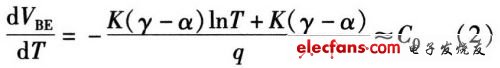
If the effect of the change in lnT term caused by temperature change on equation (2) is ignored, dVBE / dT can be approximately equal to the constant C0. At normal temperature, C0 is about -2 mV / K. In order to simplify the calculation, the change equation of PN junction with respect to temperature can be approximately linear as
![]()
The voltage at point B is the voltage on the resistor, which can be calculated by Ohm's theorem. Calculate the temperature rise flip point TH. When the temperature rises, it can be seen from the previous analysis that TSD is high and M2 is cut off. Therefore, the current flowing into R0 is only I1. The expression of VB voltage in this state is
![]()
The corresponding equation at the turning point (VA = VB) is
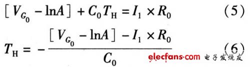
Calculate the temperature drop flip point TL When the temperature drops from above TH, it can be seen from the previous analysis that TSD is low and M2 is turned on. Therefore, the current flowing into the resistor R has two paths of I1 and I2. The expression of VB voltage in this state is
![]()
The corresponding equation when turning point (VA = VB) is
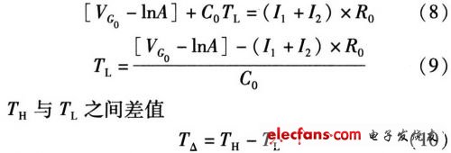
Equation (10) is the hysteresis when the over-temperature protection works.
2 Actual circuit design
The designed overheat protection circuit is roughly divided into 3 parts, as shown in Figure 2.
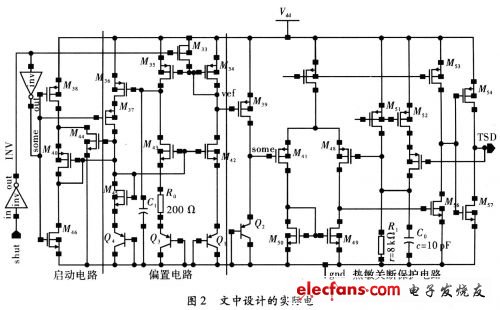
Start-up circuit: The start-up circuit will only work when power is turned on. When the power supply voltage rises slowly from 0 V and the input signal Shut is low, the switch M37 will be turned on and the MOS tube M38 will also be turned on It will make the voltage on the M38 branch rise slowly. The gate terminal of the M40 connected in the form of a diode will also increase accordingly, and also provides the gate voltage for the M45, M43, M42 on the right end, thereby disrupting the balance of the reference circuit and enabling it to start up. When the gate voltage of M40 rises to the threshold voltage of M44, it will be turned on, so that there is a path from power to ground, so that the function of starting the circuit is completed.
Bias circuit: The working principle of this part of the circuit is basically the same as that of the PTAT current circuit. The voltage at the output terminal provides bias for other circuits. The branch composed of M36, M45 and Q4 takes out the current at the right branch, filters it, amplifies it and mirrors it back, and outputs a bias voltage signal on the branch of M34, M42 and Q1. Due to the working principle of the current mirror, M34 ~ M36 and M42 ~ M45 are required to be the same pair of tubes. In addition, M33 acts as a shutdown tube in this circuit. When the Shut signal is high, M33 will be in the on state, so that this time will turn off M34, M35, so that the entire circuit is turned off.
Thermal shutdown protection circuit: Since the bias voltage output by the reference circuit is added to the gates of M39, M51, and M52, PTAT current will be generated on both branches. The two-stage comparator composed of M41, M47, M48, M49 and M50 is used to realize the function of Comp in the principle equivalent diagram. The first stage of this comparator is the PMOS differential input.
Use PMOS as a differential input: (1) Reduce the input noise. Under normal circumstances, there can be no dramatic changes in temperature, so the frequency of temperature fluctuations cannot be very high, so flicker noise 1 / f will become the main component of noise. Because the PMOS input can reduce the influence of noise on the circuit; (2) The PMOS input reduces the lower limit of the common mode input range. This circuit comparator needs to compare the voltage close to the PN junction VBE. The input terminal formed with PMOS can better meet the requirements of this low common-mode input voltage. The second stage of the comparator is a common source amplifier. As the second stage of the comparator, its main role is to increase the output swing, improve the gain and input resolution, and accelerate the conversion rate of high and low levels. The role of the capacitor C0 in the circuit: the capacitor C0 can suppress the voltage fluctuations generated by some interference quantities on the resistance wind of the comparator leading to the input terminal to prevent the malfunction caused by the disturbance of the system.
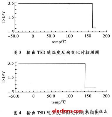
3 Simulation test
Follow the circuit designed above. It was simulated with Cadence Specture, and the model parameters of the device used 0.35μm CMOS process. Figure 2 is the curve of the output control signal TSD of the over-temperature protection circuit, with the temperature rising and falling. The power supply voltage is 3.3 V. It can be seen from the simulation results that the circuit achieves good "temperature hysteresis" characteristics. The hysteresis function effectively avoids thermal oscillation problems in the chip. Turn-off temperature TH160 ° and recovery temperature TL140 °.
4 Conclusion
The overheat protection circuit designed in this paper uses PTAT current to detect the temperature change, and converts it into a voltage signal to input two-stage comparator for comparison, thereby generating an overheat protection signal. The hysteresis effect of the comparator can effectively prevent the occurrence of thermal oscillation. The circuit has high sensitivity to temperature sensing and is very suitable for integration in integrated circuit chips.
Asic Miner Bitmain:Asic Miner Bitmain Ka3 166Th Kda Mining Machine
Bitmain is the world's leading digital currency mining machine manufacturer. Its brand ANTMINER has maintained a long-term technological and market dominance in the industry, with customers covering more than 100 countries and regions. The company has subsidiaries in China, the United States, Singapore, Malaysia, Kazakhstan and other places.
Bitmain has a unique computing power efficiency ratio technology to provide the global blockchain network with outstanding computing power infrastructure and solutions. Since its establishment in 2013, ANTMINER BTC mining machine single computing power has increased by three orders of magnitude, while computing power efficiency ratio has decreased by two orders of magnitude. Bitmain's vision is to make the digital world a better place for mankind.
Asic Miner Bitmain,Ka3 166Th Kda,Kda Miner Antminer Ka3,Asic Miner Ka3,ka3 miner
Shenzhen YLHM Technology Co., Ltd. , https://www.hkcryptominer.com