Automotive electronics are in a noisy environment, so automotive electronics must have excellent electromagnetic compatibility (EMC) performance. The most important part of the EMC design of automotive electronics is the design of the microprocessor. The author will combine the actual design experience, analyze the noise generation mechanism and propose a method to eliminate noise.
This article refers to the address: http://
Automotive electronics often work in harsh environments: ambient temperatures range from -40oC to 125oC; vibrations and shocks often occur; there are many sources of noise, such as wiper motors, fuel pumps, spark ignition coils, air conditioner starters, alternator cables Intermittent disconnection of connections, as well as certain wireless electronic devices such as cell phones and pagers.
Automotive designs typically have a highly integrated microcontroller that performs a large amount of calculations and controls the operation of the vehicle, including engine management and brake control. Automotive electronic design not only needs to protect the MCU in this noisy environment, but also must specify the MCU module design to ensure that the noise emitted by the MCU module meets the relevant specifications.
Conceptually, electromagnetic compatibility (EMC) consists of the system's own sensitivity to noise and the noise emission. Noise can be transmitted by electromagnetic fields to generate radiated interference, and can also be transmitted by parasitic effects on the chip or off-chip.
EMC is becoming more and more important in most automotive control system designs. If the system is designed to not interfere with other systems and is not affected by other system emissions and does not interfere with the system itself, then the system designed is electromagnetically compatible.
Any electronic equipment and systems sold in the United States must meet the EMC standards set by the Federal Communications Commission (FCC), and major US automakers have their own set of test specifications to constrain their suppliers. Other car companies usually have their own requirements, such as:
SAE J1113 (Electromagnetic Sensitivity Test Procedure for Automotive Devices) gives the recommended test levels and test procedures for automotive components.
SAE J 1338 provides information on how to test the electromagnetic sensitivity of the entire car.
The second and fourth parts of SAE J1752/3 and IEC 61967 are two standards dedicated to IC emission testing.
Europe also has its own standards. The EU EMC Directive 89/336/EEC came into effect in 1996, and since then the European automotive industry has introduced a new EMC Directive (95/54/EEC).
To check the sensitivity of the car to electromagnetic radiation, it should be ensured that the reference level of the entire car is limited to a rms value of 24V/m within the 90% bandwidth range of 20 to 1000MHz, and the rms value within the entire bandwidth range is 20V. Within /m. The driver's direct control of the steering wheel, brakes, and engine speed is tested during the test, and anomalies that may cause confusion to anyone else on the road, or abnormalities that the driver directly controls the car, are not allowed.
EMC design is important because the chip geometry is decreasing and clock speeds are increasing, causing the device to emit clock harmonics in excess of 500MHz. Such as Motorola's latest e500 architecture-based microcontroller MPC5500 series, the chip uses 0.1 micron process technology, the clock frequency is 200MHz.
In addition, product cost requirements force manufacturers to design boards without using formations and minimizing component count, and automotive design engineers face very stringent design constraints. The electronic system designed must be highly reliable, even if one of the one million cars has a simple fault that is not allowed. The fact that all cars were recalled without considering EMC design proves that this practice not only has a huge loss, but also affects the reputation of automakers.
In EMC design, the concept of “injured party†generally refers to those components that are affected by the lack of EMC considerations in the design. The victim component may be internal to the MCU-based PCB or module, or it may be an external system. The usual victim component is a broadband receiver in a Keyless-Entry module or a garage door opener receiver. The receivers in these modules are incorrect due to the strong enough noise from the MCU. I think I received a remote control signal.
Car radios are often also a victim component: MCUs can generate a large number of FM band harmonics, severely degrading sound quality. Other modules distributed in the car may also be similarly affected. The emission noise generated by the MCU-based module is propagated through the cable. If the MCU generates enough strong noise to interfere with text and voice, the cordless phone and pager are also vulnerable. interference.
EMC design
Many EMC design techniques can be applied to board and SoC designs. The most common part is the transmission line effect and the parasitic resistance, capacitance and inductance effects on the wiring and power distribution network. Of course, there are many technologies related to the chip itself in the SoC design, including substrate materials, device geometries, and packages.
First understand the transmission line effect. If there is an impedance mismatch between the transmitter and the receiver, the signal will reflect and cause a voltage ringing, thereby reducing the noise margin, increasing the signal crosstalk and generating signal emissions interference through capacitive coupling. The transmission line size on the IC is usually very small, so it does not emit noise or is affected by radiated noise. The transmission line size on the board is usually large, which is easy to cause. The most common solution is to use a series terminator.
In SoC designs, noise is primarily transmitted through parasitic resistance and capacitance rather than electromagnetic fields. The CMOS chip enhances the anti-locking capability by implementing an extremely low-resistance substrate by an epitaxial process, while the bottom side of the substrate provides an effective conduction path for the substrate noise, making it difficult to electrically connect the noise source to the sensitive node. Separated by.
Many parallel p+ substrate contacts provide a low impedance path for resistive coupling noise. Parasitic capacitance is formed between the sidewalls and the bottom of the n-well and p-channel transistor p substrate, thereby generating capacitive coupling noise and forming a pn junction between the base and source regions of the n-channel transistor (see Figure 1). .
The single pn junction capacitance is very small. In a VLSI SoC design, the sum of the parallel capacitors is usually a few nanofarads. Directly connect the source region to the substrate before connecting to the power network to short out the capacitor. This technique also eliminates the body effect caused by the transient negative current entering the substrate. The bulk effect increases the depletion region and causes the Vt of the transistor to go high. The same technique can be applied to n-well p-channel transistors to reduce capacitive coupling noise.
 Javascript:resizepic(this) border=0>
However, digital or analog circuits that include stacked transistors typically require isolation of the source region. In this case, increasing the capacitance of Vss to the substrate or Vdd to the substrate can reduce noise transients. For analog circuit designs, body effects reduce circuit performance by changing the bias current and signal bandwidth, so other solutions such as well isolation are required. For digital circuits, a single well is ideal for reducing the chip area. Body effects can be compensated for through careful design.
Another source of substrate noise is the impact-ionization current, which is related to the process technology, which occurs when the NMOS transistor reaches the pinch-off voltage. Collision ionization produces a hole current (positive instantaneous current) at the substrate.
In general, the frequency of the substrate noise can be as high as 1 GHz, so the skin effect must be considered. The skin effect is to guide the body to increase the inductance as the depth increases, reaching a maximum at the center of the conductor. The skin effect can cause attenuation of the on-chip signal and distortion of the signal on the p+ base layer of the chip. To minimize the skin effect, the substrate thickness is required to be less than 150 microns, which is much smaller than the minimum mechanical thickness allowed for some substrates, whereas thinner substrates are more brittle.
Noise source
There are four main sources of noise inside the microcontroller: the power generated by the internal bus and the node synchronous switch and the current on the ground; the conversion of the output pin signal; the noise generated by the oscillator operation; the on-chip signal illusion generated by the switched capacitor load .
Many design methods can reduce synchronous switching noise (SSN). Penetration current is a major source of SSN, and all clock drivers, bus drivers, and output pin drivers can be affected by this effect. This effect occurs in a complementary type of inverter, and the p-channel transistor and the n-channel transistor are simultaneously turned on at the same time when the output state changes. It is ensured that the other transistor is turned off before the complementary transistor is turned on to achieve the minimum penetration current. In the design of a high current driver, this may require a pre-driver to control the conversion rate of the node signal.
SSN can also be reduced by cutting off the clock that does not require the module. Obviously, this technology is very relevant to specific applications, and the application of this technology can improve EMC performance. In highly integrated microcontroller chips like Motorola's MPC555 and 565, peripheral modules of all chips have this capability.
SSN also produces radiated interference, and instantaneous power and ground currents flow through the device pins to external decoupling capacitors. If the loop formed by the circuit (including bonding wires, package leads, and PCB wires) is large enough, a signal emission will occur. The parasitic inductance in the loop creates a voltage drop that will further cause common mode radiated interference.
The intensity of the common mode radiated electric field E is calculated by the following equation:
E = 1.26 x 10⁻⁶ Iw fl/d
E = 1.26 x 10⁻⁶ Iw fl/d
Here, the unit of E is volts/meter, the unit of Iw is ampere, f is unit of Hertz, l is the path length, d is the distance to the path, and the units of l and d are meters. In complex designs, the frequency is determined by the specific application requirements and cannot be reduced, so SoC design engineers must seriously consider how to reduce the electric field strength by reducing Iw or l.
Handling the clock domain can also reduce the SSN. Many good SoC designs are synchronous circuits that make it easy to generate large peak currents at the top and bottom of the clock. Instead of using a large driver, the clock drivers are distributed throughout the chip, which allows the transient current to be distributed. Another possibility is to make sure that the clocks do not overlap each other. Of course, care must be taken to avoid competition due to timing mismatch. More importantly, the clock signal should be away from sensitive I/O logic signals, especially analog circuits.
Today's complex embedded MCUs have many output signals, and most of the output signals must be able to respond quickly to capacitive loads. These signals include clock, data, address, and high frequency serial communication signals. For internal nodes, both the through current and the capacitive load generate noise. Applying the same technique to internal nodes can solve the problem of output pin driver circuit noise. In addition, a fast transition of the signal on the pin can cause signal ringing and crosstalk on the output signal line caused by reflection.
There are many solutions to minimize this type of noise source. The output driver can be designed such that the drive strength can be controlled, and the signal slew rate control circuit can be added to limit the di/dt. Since most device test equipment has higher test node capacitance than the final application, it is often preferred to specify a fixed value to achieve drive strength control. For example, assume that the CLKOUT full drive strength of the MCU microcontroller series of the MPC5XX family is a 90pF load and is set for testing purposes. In addition to considering full drive strength due to timing, it is preferable to use reduced drive strength.
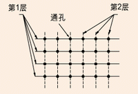
The technique described above has a positive effect on noise reduction, and the average current actually increases due to the transient envelope of the transient current. Implementing an LVDS physical layer on the chip also reduces the noise generated by large transient currents on the output pins, which relies on a differential mode current source to drive a low-impedance external load (Figure 2). The voltage swing is limited to ±300mV.
The additional pins required to support this technology can be compensated for by reducing the power pins. Since this implementation effectively reduces the on-chip transient current, the output driver maintains a constant DC current through the power supply, while conventional drivers The transient current in the current creates a large voltage swing across the capacitive load.
 Javascript:resizepic(this) border=0>
There are two aspects in the oscillator design that affect EMC: the shape of the input and output signal waveforms has an effect; the ability to achieve spectral broadening and reduce its narrowband power through frequency jitter.
Oscillator is essentially an analog circuit and is therefore more sensitive to process, temperature, voltage, and load effects than digital circuits in SoC. Limiting the oscillator signal amplitude using feedback in the form of an automatic gain control (AGC) circuit can eliminate most of these effects. Another alternative to AGC is the dual mode oscillator, which switches between high current mode and low current mode. In the initial state, the high current mode is used when the power is turned on to ensure a short start-up time, and then switching to the low current mode ensures minimum noise.
In SoC designs that integrate a phase-locked loop that is part of the oscillator circuit, the frequency jitter can be used to vary the clock frequency over a small range, so that as the frequency spreads over a range, the fundamental energy can be reduced. The entire system design must be carefully considered to ensure that the ratio of such changes and the frequency range do not affect the timing of critical components in the final application. This method cannot be adopted in serial communication such as CAN, asynchronous SCI, and timing I/O functions, which are widely used in automobiles. The switching noise on the chip indicates that it is a damped oscillation of the desired signal output, which is the result of the series combination of the inductor and the load capacitance on the chip. For a typical on-chip bus, the load is a long PCB trace connected to a number of tristate buffers. The body of the load is a capacitor, including the gate, pn junction, and interconnect capacitor.
Eliminating inductance or reducing di/dt can reduce or eliminate noise. It is only necessary to carefully consider the noise problem in the design when the noise amplitude is so large that it will cause the connection section error switch.
Reducing sensitivity to external noise sources includes consideration of external devices and internal design. External transient currents can cause two conditions on the pin: voltage changes can cause capacitively coupled currents to enter the device; voltages outside the supply range will eventually conduct current through the resistive path into the device.
In automotive electronics design, an external RC filter is typically used to limit transient voltage swing and injection current. Care must be taken to ensure that external device values ​​take into account leakage current effects, especially at analog inputs. It is worth noting that the MCU and peripheral ICs typically have up to 200 I/O pins. The extra cost and board space required for this solution make engineers reluctant to adopt them in system design. The best solution is to achieve a high level of integration on the chip.
Hardware and software technologies can work together to achieve EMC performance requirements. For example, many MCUs have the ability to output internal access on an external bus, which is usually invisible. This approach is very useful for debugging, but there may be external bus contention in some poorly designed systems, which increases the associated noise.
In the past work I have encountered a similar problem with incorrect reading of the A/D converter on the chip. It seems that the noise interferes with the measurement or the transformation to some extent. By understanding the hardware structure of the system, it seems that everything is normal from the surface of the input part of the A/D converter, but I noticed that the external EPROM is decoded in some way, and this decoding method is very special. In this case, the bus competition may be caused. This kind of competition will not affect any operation of the program, but it will generate enough noise, so there will be an accidental A/D conversion error. This problem was quickly solved by changing the decoding logic.
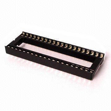
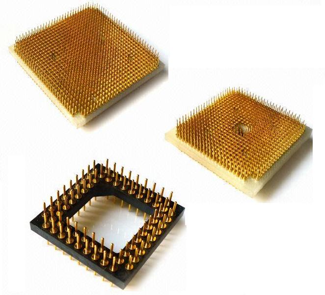
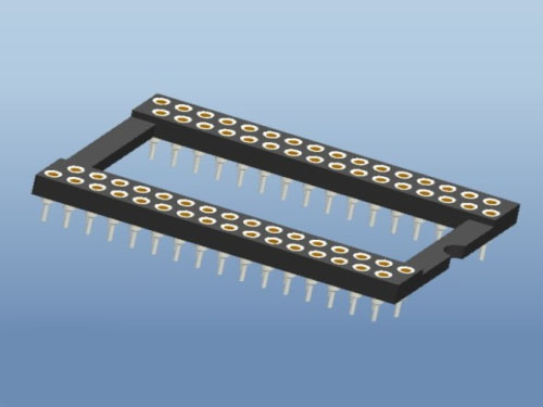
1.ANTENK Tech ICS Series Ic Sockets are a low profile design available in single or dual row in .100" centerline pin spacing with .300" or .600" row spacing. Our ISD Series .are fine pitched sockets on 0.070" centerlines with .300" or .600" row spacing. All Adam Tech sockets are manufacured with our exclusive single beam dual wipe contact design which produces a high pressure wiping action for superior connectivity. In addition to an internal contact stop which prevents over stressing of the contact, each has a wide lead in to eliminate mis-mating and a closed bottom anti-solder wicking design.
2.Our products are widely used in electronic equipments,such as monitors ,electronic instruments,computer motherboards,program-controlled switchboards,LED,digital cameras,MP4 players,a variety of removable storage disks,cordless telephones,walkie-talkies,mobile phones,digital home appliances and electronic toys,high-speed train,aviation,communication station,Military and so o
TECHNICAL SPECS:
Current Rating: 1.0Amp
Contact Resistance: 20MΩ max
Dielectric Strength: Min 1000 V RMS
Mechanical Life: Min 100 cycles
Insulation Resistance: 1000MΩ Min
Operating Temperature: -55°C to +125°C
Contact: Bronze,Tin plating
Contact Plating: Au or Sn Over Ni
Insulator Material: PPS+30%GF UL 94V-0
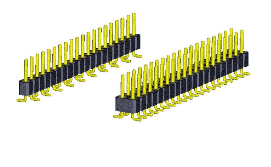
SPECIFICATIONS:
Insulator: PPS
Fiammability: UL 94V-0
Sleeve: Brass
Mating pin ∅: 0.41 mm
Mechanical life: min 500 cycles
Rated cument: 1A
Contact resistance: max 10 mΩ
Dielectric strength: min 1000V RMS
Ic Sockets,Ic Socket Connectors,Pin Ic Socket,Pin Ic Socket Connector
SHENZHEN ANTENK ELECTRONICS CO,LTD , http://www.antenk.com