FPGA (Field-Programmable Gate Array), which is a field-programmable gate array, is a product further developed on the basis of programmable devices such as PAL, GAL, and CPLD. It emerged as a semi-custom circuit in the field of application specific integrated circuits (ASIC), which not only solves the shortcomings of the custom circuit, but also overcomes the shortcomings of the limited number of original programmable device gates. The development of FPGAs is quite different from the development of traditional PCs and microcontrollers. FPGA is mainly based on parallel computing and implemented in hardware description language. Compared with PC or single-chip microcomputer (whether von Neumann structure or Harvard architecture), the sequential operation is very different, which also makes FPGA development difficult. Here are a few sets of schematic designs for everyone:
Reset and crystal circuit schematic designA chip, especially a programmable chip, usually requires a short period of time to initialize internal parameters at the moment of power-on. At this time, the chip cannot enter the working state immediately. It is usually said that the power-on initialization is a reset, and the circuit that performs this function is called a reset circuit. This FPGA chip uses a low level reset, supports power-on reset and manual reset, and generates a low level after RESET is pressed.
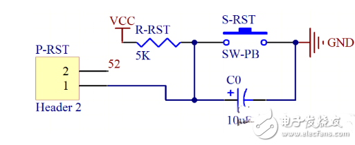
Reset circuit schematic design
Crystal circuit schematic designThe crystal oscillator is a component that provides a frequency reference for the circuit. It is usually divided into two major categories: an active crystal oscillator and a passive crystal oscillator. The passive crystal oscillator needs an oscillator inside the chip, and the signal voltage of the crystal oscillator is determined according to the oscillating circuit, allowing different Voltage, but passive crystal oscillators usually have poor signal quality and accuracy. They need to accurately match peripheral circuits (inductors, capacitors, resistors, etc.). If you need to replace the crystal oscillator, you must replace the peripheral circuit at the same time. The active crystal oscillator does not require the chip's internal oscillator and provides a high-precision frequency reference with better signal quality than passive crystals. This FPGA chip uses a 50 MHz active chip crystal as the clock input for the chip operation.
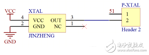
Crystal oscillation circuit schematic design
A key switch circuit schematic designThe four-legged buttons used on the minimum system board are actually divided into two groups, two of which are connected, and the two groups directly control the on-off state through the above buttons. Simply understand that the switch is OK, press the two ends to form a short circuit, and release the hand to form an open circuit. A short circuit is equivalent to input 0 and an open circuit is 1. In addition, it should be noted that since the button belongs to the mechanical switch, there is inevitably a jitter phenomenon when the button is pressed, so the time for the user to press the button can be slightly longer.
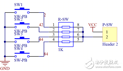
Key switch circuit schematic design
Eight-digit dial switch circuit schematic designThe DIP switch is equivalent to a switch quantity. When it is turned ON, it means ON, OFF is OFF, in the digital circuit, 0, 1, it is usually used for binary input. The minimum system board of this topic uses an eight-digit DIP switch as a byte input. When it is turned ON, it is equivalent to input “1â€, and the default input is “0â€.
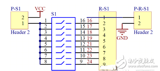
Eight-digit dial switch circuit schematic design
Overall circuit schematic for minimum system circuit designUsing the circuit schematics designed by AlTIum software, the FPGA minimum system board includes a clock circuit, a reset circuit, a power supply circuit, a JATG circuit, a PROM configuration circuit, a display module circuit, a switch circuit, and various interface circuits.
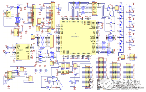
Overall circuit schematic for minimum system circuit design
The application fields of FPGA products have expanded from the original communication to a wide range of fields such as consumer electronics, automotive electronics, industrial control, and test and measurement. Applying relatively mature technology to certain specific fields such as communication, video, information processing, etc. to develop products that meet the needs of the industry and can be accepted by industry customers. This is mainly a combination of FPGA technology and professional technology. Interface problems with professional customers Product design also includes professional tool products and civilian products. The former focuses on performance, while the latter focuses on price-sensitive product design to achieve product functionality. FPGA technology is an implementation means in this field, FPGA because Features such as interface, control, function IP, embedded CPU, etc. Conditional realization of a simple structure, high degree of curing, full-featured system product design will be the most widely used market for FPGA technology, with a huge explosive demand space product The design has high requirements for technicians and the road is long. However, the whole industry is now in the state of forming a “first teamâ€. As long as it is added, the future product design is a career development orientation, not a simple hobby. Arrived! The product design field will create a large number of enterprises and entrepreneurs, which is a development hotspot and opportunity.
Pearl Cotton Bag Cutting Machine
Pearl Cotton Bag Cutting Machine,Front Sealing Bag Cutting Machine,High-Speed Bag Cutting Machine,Square Bottom Bag Cutting Machine
Dongguan Yuantong Technology Co., Ltd. , https://www.ytbagmachine.com