VGA (Video Graphics Array) is the video graphics array, which is the meaning of IBM with PS / 2 in 1987 (PS / 2 was originally "Personal System 2", "Personal System 2" is a kind of IBM launched in 1987 Personal computer. The keyboard and mouse interface used on the PS / 2 computer is the current PS / 2 interface. Because the standard is not open, the PS / 2 computer has failed in the market. Only the PS / 2 interface has been used until today). A video transmission standard for analog signals at the time had the advantages of high resolution, fast display rate, and rich colors, and was widely used in the field of color displays. This standard is very outdated for today's personal computer market. Even so, VGA is still a standard commonly supported by most manufacturers, and personal computers must support the VGA standard before loading their own unique drivers. For example, the startup screen of Microsoft Windows series products still use VGA display mode, which also shows its importance and compatibility in the display standard.
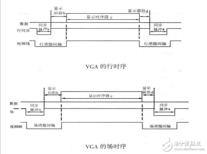
VGA timing standardThe time to complete one line of scanning is called horizontal scanning time, and its reciprocal is called line frequency; the time to complete one frame (full screen) scanning is called vertical scanning time, and its reciprocal is called field frequency, which is the frequency of refreshing a screen. There are 60Hz, 75Hz, etc. The standard VGA display has a field frequency of 60Hz and a line frequency of 31.5KHz.
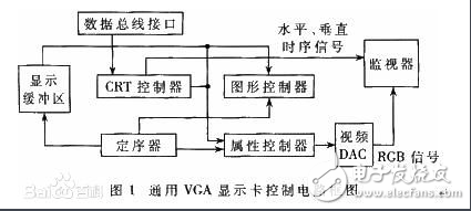
The general VGA display card system is mainly composed of three parts: control circuit, display buffer and video BIOS (Basic Input Output System) program. The control circuit is shown in Figure 1. The control circuit mainly completes functions such as timing generation, data operation of the display buffer, master clock selection, and D / A (Digital to Analog converts digital signals to analog signals) conversion; the display buffer provides display data buffer space; and the video BIOS as the control program It is solidified in the ROM (Read-Only Memory) of the display card.
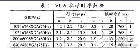
Through the analysis of the basic working principle of the VGA display card, we can know that to realize the VGA display, we must solve the problems of data source, data storage, and timing implementation. The key is how to realize the VGA timing. VGA's standard reference display timing is shown in Figure 2. Both line timing and frame timing need to generate four parts: sync pulse (Sync a), display back edge (Back porch b), display timing segment (Display interval c) and display front edge (Front porch d). The timing parameters of several common modes are shown in Table 1.
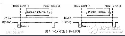
First, determine the main clock frequency according to the refresh frequency, and then calculate the total number of line cycles from the main clock frequency and image resolution, and then according to the main count pulse source for the timings of the a, b, c, and d timing sections given in Table The frequency is converted to the number of clock cycles. Use counters and RS flip-flops in CPLD to generate pulse signals of different widths and cycles based on the calculated clock cycles of each timing segment, and then use their logical combination to form a, b, c, d in Figure 2 The blank signal BLANK and the synchronization signal SYNC of each timing segment and the D / A converter.
SRAM address
The main clock is used as the pixel count pulse signal, and provides the read signal of the memory SRAM and the D / A conversion clock. The output of the counter driven by it is used as the low address of the read SRAM. The line synchronization signal is used as the line count pulse signal, and the output terminal of the counter driven by it is used to read the high-order address of the SRAM. Since two SRAMs are used, the most significant address is used as a chip select for SRAM. Because there is a certain time delay when the signal passes through the CPLD internal logic device, when the CPLD generates the address and read signal to read the data, the read signal, address signal and data signal cannot meet the timing requirements of the SRAM read data. You can use the hardware circuit to perform certain timing adjustments on the read signal, so that each signal can meet the timing requirements of reading SRAM and inputting data for the DAC.
dataIf the VGA displays a true-color BMP image, then each of the three components of R, G, and B needs 8 bits, that is, 24 bits represent a pixel value, and in many cases 32 bits are used to represent a pixel value. In order to save the storage space of the video memory, a high-color image can be used, that is, each pixel value is represented by 16 bits, and the three components of R, G, and B use 5, 6, and 5, respectively, which is half of the data amount of the true color image , And at the same time can meet the display effect.
Home Appliances Wire
We supply rigorous UL standard electronics wires used in internal wiring of home appliances and electrical equipment such as air conditioner, humidifier, washing machine, fridge, rice cooker, microwave etc. Insulations include PVC, SXL(XLPVC), silicone rubber and FEP with the heat resistance from 176°F(80°C) to 392°F (200°C). Feyvan electronics has carried R&D on covering materials for many years, even some special Insulation materials such as TPE, TPU, insects prevention and rats prevention, our engineers have much experience to provide professional solutions for you.
Home Appliances Wire,Electrical Panel Wiring,Home Wiring,Home Electrical Wiring
Feyvan Electronics Technology Co., Ltd. , https://www.fv-cable-assembly.com