Introduction: Many people find it difficult to switch power supply, but it is not. It is not difficult to design a switching power supply. It is difficult to do fine work. When you really get started, it is much simpler to accumulate certain experience and then use discrete structure to design. Everything is difficult at the beginning, and the author is here to introduce jade and slowly explain how to design the switching power supply step by step.
The first step in the design of the switching power supply is to look at the specifications. Many people have contacted it. It can also be proposed for your reference. I will help with the analysis.
I only bring you a wide range of input, 12V2A conventional isolated switching power supply.
1. First determine the power , according to the specific requirements to select the corresponding topology; such a switching power supply multi-select flyback can basically meet the requirements. Here I will choose more empirical formulas for calculation. If there is a need for analysis, I can come up with it and discuss it.
2. Select the corresponding PWMIC and MOS for preliminary circuit schematic design
When we decided to design with the flyback topology, we needed to select the corresponding PWMIC and MOS for the preliminary schematic design (sch). Whether you choose to use discrete or integrated, you can consider it yourself. I will also break down the calculations inside.
Discrete: PWMIC and MOS are separate. This advantage is that the power can be freely matched. The disadvantage is that the design and debugging cycle will be longer (only from the design point of view); integrated: the PWMIC and MOS are integrated in one In the package, it saves the designer a lot of calculation and debugging steps, suitable for the environment just getting started or fast development.
  3. Do the schematic
After determining the selected chip, I started to make the schematic (sch), where I chose STVIPer53DIP (integrated MOS) for design.
It is best to look at the corresponding datasheet before designing to confirm the simple parameters. Whether you choose PI integration, or separate 384x or OBLD, you need to refer to the datasheet. The general datasheet will be accompanied by a simple circuit schematic, these schematics are our design basis.
  4. Determine the corresponding parameters
After we complete the schematic, we need to determine the corresponding parameters to enter the next PCBLayout. Of course, different companies have different processes, we need to follow the corresponding process and develop a good design habit. This step may have preliminary evaluation, schematic confirmation, etc. After the signing is completed, it can be calculated.
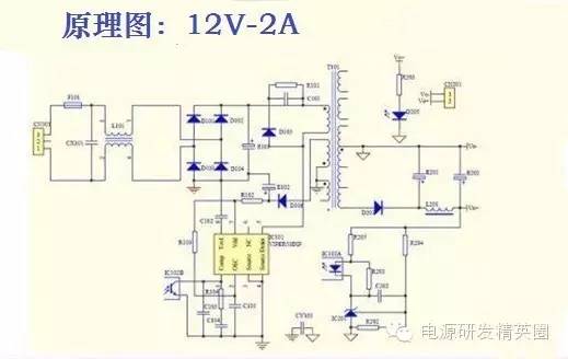
Attach the corresponding schematic diagram first.
5. Determine the switching frequency and select the core to determine the transformer
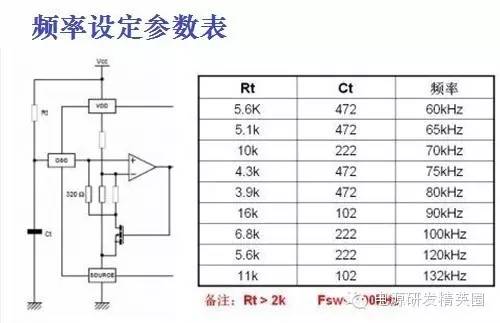
Here, it is determined that the chip operating frequency is 70KHz, the frequency of the chip can be set by the external RC, and the working frequency is equal to the switching frequency. The function of this peripheral is beneficial to us to design the switching power supply better, and can also adopt the external synchronization function. Similar to the UC384X function.
The transformer core is EER28/28L.
Generally AC2DC converter, the operating frequency should not be set more than 100kHz, mainly because the frequency of the switching power supply is too high, which is not conducive to the stability of the system, and is not conducive to the passability of EMC. The frequency is too high, the corresponding di / dtdv / dt will increase, in addition to the working frequency of PI132kHz, you can refer to other chips, you will summarize your experience.
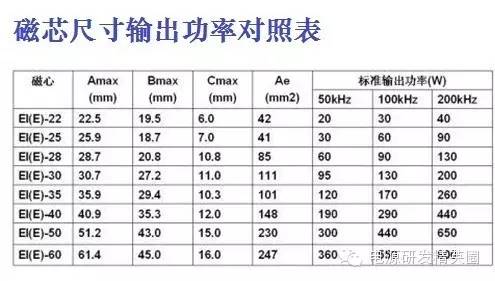
For the selection of the core, it is based on the switching frequency and power, and more is the experience selection. Of course, you need to get more core parameters, including magnetic material, Curie temperature, frequency characteristics, etc., which needs to be built slowly.
EE25EER25EER28EFD25EFD30 can be used in the range of 20W~40W.
About the choice of transformer core
Power size:
Cores that can be used less than 5w:
ER9.5, ER11.5, EE8.3, EE10, EE13, RM4, GU11, EP7, EP10, UI9.8, URS7
5-10W usable core:
ER20, EE19, RM5, GU14, EFD15, EI22, EPC13, EF16, EP13, UI11.5
10-20W usable core:
ER25, EE20, EE25, RM6, GU18, EPC17, EF20
20-50W usable core:
ER28, ETD28, EI28, EE28, EE30, EF25, RM8, GU22,
PQ20, EPC19, EFD20
50-100W usable core:
ER35, ETD34, EE35, EI35, EF30, RM10, GU30, PQ26,
EPC25, EFD25
100-200W usable core:
ER40, ER42, ETD39, EI40, RM12, GU36, PQ32, EFD30
200-500W usable core:
ER49, ETD49, EC53, EE42, EE55, EI50, RM14, GU42,
PQ35, PQ40, UU66
Magnetic cores larger than 500W:
ER70, ETD59, EE65, EE85, GU59, PQ50, UU80, UU93
Core and transmission power comparison table
6. Design the transformer for calculation
Input input: 85~265Vac
Output output: 12V2A
Switching frequency Fsw: 70kHz
Core core: EER28/28L
Core parameters: Ae82mm2
All of the above are known parameters, we also need to set some parameters, you can enter the next calculation.
Setting parameters:
Efficiency η=80%
Maximum duty cycle: Dmax=0.45
Magnetic induction change: ΔB=0.2
With these parameters, we can calculate the number of turns and inductance.
Output power Po=12V*2A=24W
Input power Pin=Po/η=24W/0.8=30W
Input minimum voltage Vin(min)=Vac(min)*sqr(2)=85Vac*1.414=120Vdc
Input the highest voltage Vin(max)=Vac(max)*sqr(2)=265Vac*1.414=375Vdc
Input average current Iav=Pin/Vin(min)=30W/120Vdc=0.25A
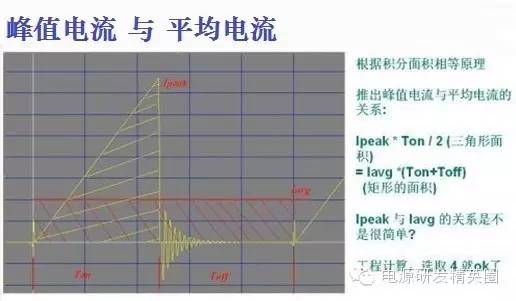
Input peak current Ipeak=4*Iav=1A
Primary inductance Lp=Vin(min)*Dmax/(Ipeak*Fsw)=120Vdc*0.45/(1A*70K)=770uH
The 4 here is an experience value and of course my own exclusive experience. As for the derivation, don't bother, look at the picture below, you will understand, the following is the current waveform of DCM; as for the CCM plus a platform, you can derive it, very simple.
At this most important step, the primary inductance has been obtained. For leakage inductance and air gap, I do not recommend that you calculate and verify.
Leakage feeling Lleakage<5%*Lp
The inductance of the transformer is calculated above, and now we need to get the corresponding number of turns to complete the operation of the entire transformer.
1) Calculate the on-time Ton cycle time T=Ton+Toff=1/FswTon=T*DmaxFsw, Dmax is a known amount of 70 kHz, and 0.45 is substituted into the above formula to obtain Ton=6.43us
2) Calculate the primary turns of the transformer Np=Vin(min)*Ton/(ΔB×Ae)=120Vdc*6.43us/(0.2*82mm2)=47T (the number here must be rounded, and it is rounded up) , our transformer can not only be half a circle or other non-integer circle)
3) Calculate the number of turns output voltage (Vo) of the main output of the transformer 12V:
12Vdc rectifier tube pressure drop (Vd): 0.7
Vdc winding voltage drop (Vs): 0.5
Vdc primary side undulation ratio (K)=Vi_min/Np=120Vdc/47T=2.55 output turns (Ns)=(output voltage (Vo)+rectifier pressure drop (Vd)+winding voltage drop(Vs))/original Side undulation (K) = (12Vdc + 0.7Vdc + 0.5Vdc) / 2.55 = 6T (rounded)
4) Calculate the number of turns of the auxiliary winding of the transformer (auxturning). The calculation method is the same as the output of the 12V main winding. Since the STVIPer53DIP secondary side feedback needs to be lower than 14.5Vdc, 12Vdc is selected as the auxiliary voltage. Na=6T to this step, we basically The main parameters of the transformer are obtained: primary inductance: 47T primary inductance: 0.77mH leakage inductance <5%*0.77mH=39uH12V output: 6T auxiliary winding: 6T Next we only need to resistance the winding diameter of the winding Pressure and other safety requirements, can be sent to the transformer factory to proof the air gap calculation, and return verification Dmax These are some textbooks, do not recommend that you die hard, flexible.
After calculating the number of turns above, the thickness of the enameled wire can be directly determined without complicated calculations.
The wire diameter is the same as the conventional resistance, and there are several commonly used fixed value diameters. Here, the primary current is relatively small, and φ0.25 one strand can be directly selected. The auxiliary winding is φ0.25. The main output winding φ0.4 or 0.5 three strands, do not choose to be thicker, otherwise the winding, the hardness of the enameled wire will make it difficult for the operator to wind.
After many of the "calculations" of this step have passed, the calculation will be returned to verify the window area of ​​the transformer. Personally think that return verification is superfluous, because if you can't get it, the proof transformer factory will give you feedback, and if you pass the verification, it will not necessarily pass in practice; after all, with the proficiency in the actual winding process, And sparse still has a lot to do with.
In the next step, you need to determine the size of the input and output capacitors, you can layout and layout.
7. Input and output electrolytic capacitor calculation
Input filter electrolytic capacitor
Cin=(1.5~3)*Pin
Output filter electrolytic capacitor
Cout=(200~300)*Io
Above we calculate the input power 30W
So Cin=45~90uF
In theory, the larger the value is selected, the better it will be for the latter stage; from the perspective of cost, we will not choose large capacity without limit. The value chosen here is 47uF/400Vdc85°C or 105°C depending on the application environment; the capacitor does not need high frequency, and ordinary low impedance can be used.
The output current is 2A;
Cout=400~600uF
Here, the capacitor needs to adapt to the characteristics of high frequency and low resistance. This value can also be selected to be larger, but the premise must be in the feedback loop. Because it is closed-loop precision control, it takes 470uF/16Vdc
Here, the power supply can select two 470uF/16Vdc, plus one L, which is blocked into a CLC low-pass filter.
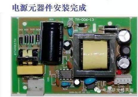
Basically, here, the device that needs shape determination on the PCB has been completed, that is, the PCB package is completed; the next step is to define the device package through the previous schematic (SCH).
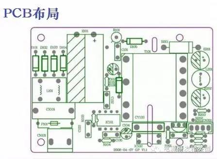
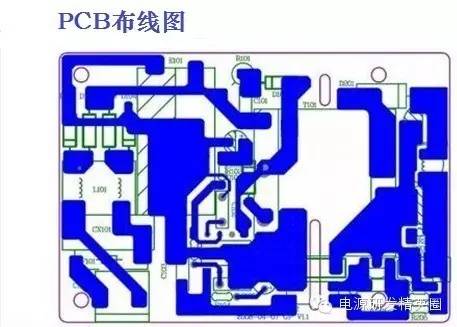
8.PCBLayout
The transformer, schematic, and electrolytic capacitor have been identified above, and the rest are basically standard parts.
Generate a network table by sch, define the board edge in the PCBfile and then load the corresponding package library, you can directly import the network table and layout; because this board is relatively simple, you can also directly deploy the board. Importing the network table is very good. Design habits.
The focus of PCBlayout is not how to connect, the most important thing is how to layout; in general, if the layout is OK, the drawing board will be much easier.
In terms of layout and layout:
1) The area of ​​the ring formed by the RCD absorbing part and the transformer is as small as possible; this can reduce the corresponding radiation and conduction.
2) The ground wire should be as short and wide as possible to ensure that the corresponding zero level is conducive to the stability of the reference; at the same time, VIPER53DIP is an important channel for the heat dissipation of the DIP-8 chip.
3) Where the di/dtdv/dt change is relatively large, minimize the loop and widen the trace to reduce unnecessary inductance characteristics.
Attached to the corresponding map, N long before the version, there are many places to improve, you can refer to yourself: the board is still in production.
9. Determine some parameters
We have already calculated the transformer in the first few steps. After the PCBLayout is completed, we can determine the same name of the transformer, define the transformer completely, and send it to proof or wrap it ourselves.
EER28/28L skeleton is 6+6
Primary side: 1->3 auxiliary: 6->5 output: 7,8,9->10,11,12
For the output of the pin, we can use two, or all use, to see your own choice.
From the schematic diagram and the PCB diagram, 1, 6, 7, 8, and 9 are the same name ends. When winding themselves, the starting line needs to be wound from the same position and wound in the same direction.
The transformer is officially defined:
1->2: φ0.25x1x24T
7->10: φ0.50x2x6T
8->11: φ0.50x2x6T
9->12: φ0.50x2x6T
2->3: φ0.25x1x23T
6->5: φ0.25x1x6T
2, 4 and cut the feet
L1-3: 0.77mH0.25V@1kHz leakage inductance is less than 5% magnetic material: PC40 or equivalent material
high pressure:
Primary side vs secondary side: 3750Vac@1mA1min without breakdown without flying arc
Secondary side vs core: 1500Vac@1mA1min without breakdown without arcing
impedance:
Primary side vs secondary side / winding vs core: 500Vdc impedance > 100M
Remarks: The sandwich wrap method is used here to reduce leakage.
All pins are output for the purpose of not wasting and reducing the internal impedance of the output winding. The PCB and the transformer can be sent out for proofing, and the rest is to determine more parameters and prepare.
D101~D104: Iav=0.25A select 1N4007 (1000V@1A) Of course, there is no problem with 600V.
Snubbercircuit (RCD absorption): R101-100k1WC101-103@1kV (high voltage ceramic capacitor)
D105-FR107 (optional 600V ultra fast recovery is also available):
This part can be calculated, or you can directly select the classic parameters. When debugging, continue to check.
D201: MBR10100
Withstand voltage:>Vo+Vin(max)*Ns/Np=12V+375Vdc*6/47=60V
D106: FR107 (withstand voltage calculation is the same as above, FR101 can also be selected, as soon as possible, the device in the power supply is integrated, so FR107 is selected)
R102: is a voltage divider resistor, mainly used to limit the voltage of Vdd; select from 0 to 100R, when debugging, adjust according to specific conditions
R103, C105: This part is the setting frequency of STVIPER53DIP, 70kHz can check the frequency setting table in the datasheet, we can know R103-10kC105-222
R103 and C105 form an RC network, which is used to set the operating frequency of VIPer53. It can work up to 300kHz, but I don't recommend using it at AC-DC. There is a curve in the VIPer53datasheet, but it is not very convenient. I will sort out the commonly used frequency setting table and post it for your reference.
The 8-pin TOVL is a delay protection. Here you can directly select 104 specific parameters and adjust this value according to the application.
The 1-pin comp is a compensation feedback pin that gives a set of verified parameters: R104-1k
C104-47uF/50V (electrolytic capacitor) C103-104 This is a first-order inertia link. In the secondary side feedback state, the compensation network based on the secondary side feedback is dominant, and the compensation network becomes the main network after the feedback is lost.
IC102-Select PC817C is OK, no need to ask for too high CTR value.
The L201-10uH3A I-shaped inductor forms a low-pass filter with the E201E202, which can better suppress the ripple. It can be calculated. I don't recommend it here for calculation. It can be adjusted according to the problems encountered in debugging.
IC201-TL431TO92 package, ref-2.5V
Calculation of the value of R205-1k>Vo-Vopdiode (pressure drop of the light-emitting diode in the photocoupler) /Imin (minimum breakdown current of the photocoupler LED)
Ensure that the R205 is selected to effectively break through the LEDs inside the optocoupler under normal conditions.
R204R202-18k4.7k can be calculated according to the formula 2.5V/R202=Vo/(R202+R204).
C202-104 can also be adjusted according to the actual situation, and there is no need to use formulas for complex calculations.
CY103- This is the Y capacitor can be selected 222@400Vac, according to the pressure tolerance of the safety regulations, can be adjusted in the subsequent work.
10. Commissioning process
To the above part, basically one power supply is designed to be completed, and the latter is the welding board debugging process.
Simple equipment required for commissioning (required): voltage regulator, oscilloscope, multimeter; auxiliary equipment: power meter, LCR bridge, electronic load
After the plate is welded, static inspection is carried out. If there is an LCR bridge, you can first measure the transformer with the same name, inductance and other parameters before soldering.
Static inspection: mainly depends on whether there is no virtual welding, even tin, etc.; after static testing, you can use a multimeter to measure the input, whether the output is in a short-circuit state; the rest can be tested for power-up.
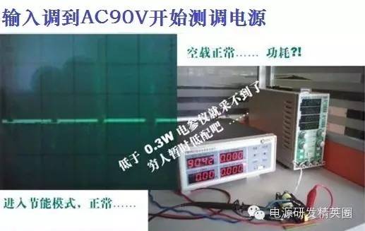
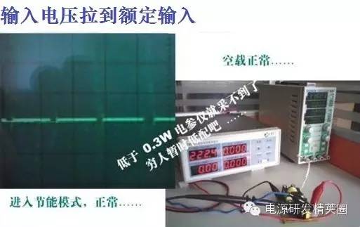
The AC input of the switching power supply is connected to the voltage regulator, or the AC input is connected to the power meter and then connected to the voltage regulator, the voltage regulator is at 0Vac; the oscilloscope is connected to the DS of the STVIPER53DIP or both ends of the primary winding, and is AC coupled; The multimeter voltage measurement output is unloaded.
Turn on the regulator power supply, start boosting, and don't need to be fast, while watching the oscilloscope.
Starting from 0Vac, you will see that the waveform on the oscilloscope will float (changing to DC coupling will make it clear that the voltage is rising). When the voltage of the regulator reaches the range of 40 to 60Vac, if the waveform of the oscilloscope has not changed, return to 0Vac and check the power board again.
Generally, the no-load state, when the range is 40 to 60Vac, the switching power supply will start to work, and the STVIPER53DIP will enter the working mode. The Vds waveform on the oscilloscope will start normal.
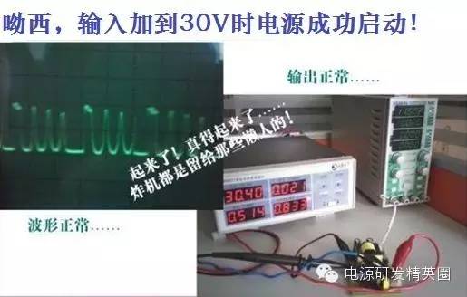
See if the output voltage reaches the preset value? Not reached, return 0Vac to check the sample, feedback and output loop. If both are OK, consider increasing the input voltage to 220Vac. If you follow the above steps to debug, there will be no explosion or bombing.
Note: The oscilloscope needs to be isolated, or only the LN input is allowed. The PE line cannot be connected without isolation, otherwise it will easily cause a short circuit.
An exciting moment has arrived, and the first power source of life will be born!
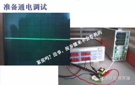
It is recommended to load it a little bit and monitor the oscilloscope. This saves the step-by-step loading process and starts directly.
Final summary:
In fact, the introduction of switching power supply is very simple, the best entry is to use a single chip, after all, the elimination of starting resistors, current detection resistors, MOS and drive, protection circuits and other uncertain factors. When you really get started, accumulate a certain amount of experience, and then use a separate structure to design is much simpler.
Solid State Relay,Relayrelay Electrical,Motor Overload Relay,Dc Coil Contactor
NanJing QUANNING electric Co.,Ltd , https://www.quanningtrading.com