Fiber optic gyro is a kind of laser gyro, which is the product of the close combination of inertial technology and optoelectronic technology. It uses the Sagnac interference effect to form a ring-shaped optical path with an optical fiber, and detects the phase difference between the two super-radiative beams generated by the rotation of the fiber ring, thereby calculating the angular velocity of the rotation of the fiber ring. The fiber optic gyroscope is mainly composed of two parts. The modulation and demodulation circuit that is servoed to the meter head is subjected to corresponding transformation to form a feedback signal to be sent to the phase modulator of the meter according to the input electrical signal. In the actual application process, the corresponding modulation and demodulation circuit should make corresponding changes according to temperature, vibration, etc., in order to maximize the accuracy requirements of the gyro. This paper designs an FPGA-based test system to simulate the head of a fiber optic gyroscope and detect the performance of the modulation and demodulation circuit.
The basic principle and structure of the analog headThe main function of the meter head is to convert the phase change caused by the optical path difference generated by the Sagnac effect into a change of optical power through the loop coupler, and then output it to the modulation and demodulation circuit in the form of an electrical signal after being detected by the detector. The structure of the digital closed-loop fiber optic gyroscope system is shown in Figure 1. The original parameter value sampled from the modulation and demodulation circuit is processed by the digital signal in the analog header to restore the actual header signal of the input modulation and demodulation circuit. After the initial reduction value is obtained, the corresponding performance index in the modulation and demodulation circuit is detected by modifying and loading different types of parameter values ​​in the analog header.
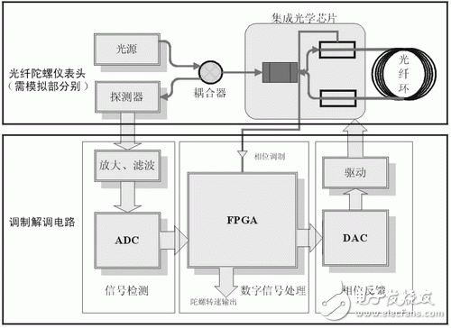
Figure 1 Digital closed-loop fiber optic gyroscope system structure
The analog head system designed in this paper follows the basic principle of the general digital closed-loop fiber-optic gyro system, and has changed in the system structure. The modem circuit is in a passive position in the system, and the header acts as the main body of the system. At the same time, the head portion of the fiber optic gyroscope was replaced by a self-designed circuit system. The structure of the analog head and its test system is shown in Figure 2.
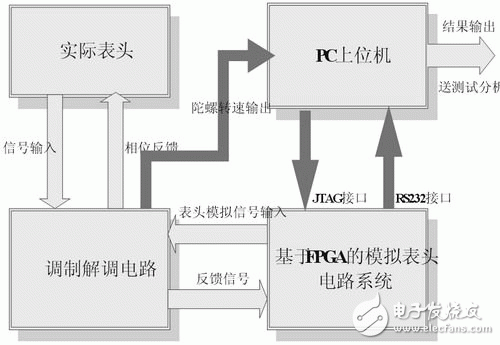
Figure 2 Analog header and its test system block diagram
In the figure, the work of the PC host computer is very important. It not only controls the cooperative work of the modulation and demodulation circuit and the analog head system, but also analyzes and organizes the collected data and completes the key software writing and implantation work.
Hardware design of analog head systemAccording to the theoretical analysis, this paper designs an FPGA-based analog header hardware system, as shown in Figure 3.
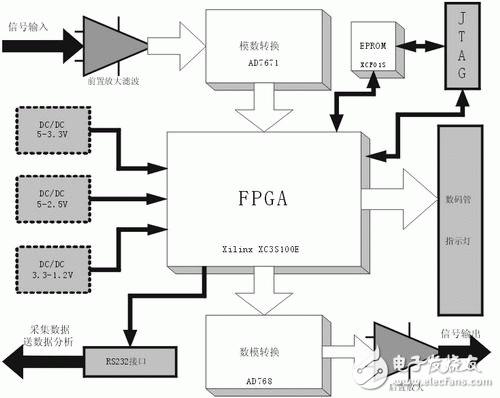
Figure 3 FPGA-based fiber optic gyroscope analog head hardware connection diagram
In this closed loop system, the main signal that needs to be acquired is the phase feedback signal in the modulation and demodulation circuit. According to the characteristics of the feedback signal, an FPGA with a small amount of computation but a fast processing speed is selected as the main component of signal processing. In this scenario, the XC3S100E FPGA chip is selected considering the cost and actual computation.
The system is powered by a ±5V regulated DC power supply. After calculation, the power consumption of the system is below 5W, so the output current of the DC power supply needs to reach 1A. According to the power supply requirements of the FPGA and its peripheral circuits, three DC/DC modules need to be set: 5V to 3.3V, 5V to 2.5V, and 3.3V to 1.2V. The MAX651, ADP3333, and LTC3406 were selected for voltage conversion. In addition, the 3.3V power supply is also used to drive ADCs, digital tubes, operational amplifiers and other devices.
The XC3S100E chip has a good price/performance ratio. It has 2,160 logic cells and 100,000 system gate resources. The maximum number of I/O ports is 108. For this system, it can fully meet the interface requirements of 16-bit input/output, digital tube indicator and other display modules, communication with the host computer and other control signals. An EPROM-XCF01S matching the FPGA is additionally configured in the system to provide loading of the target program of the logic chip after booting.
The A/D and D/A conversions use the AD7671 and AD768 chips respectively. The AD7671 has a sampling rate of up to 1MSPS, a high-speed, high-precision, parallel-transferred analog-to-digital converter with up to 16-bit resolution, and no missing codes. The maximum integral nonlinearity error (INL) is only ±2.5. LSB can meet the requirements of this system well. The AD768 is a high speed DAC with 16-bit accuracy and up to 40MSPS sample rate. Its response time is very short, the conversion speed is fast and it has a strong adaptability to high speed ADC.
When extracting the initial parameters, considering that the gyro signal is weak, the design before the A/D conversion uses the weak signal detection method to filter, shape and amplify the signal, and extract the original signal under the premise of ensuring no distortion to the maximum extent. Come out and convert to a signal output that the ADC can resolve.
Software design of analog head systemAccording to the basic principle of the closed-loop fiber optic gyroscope instrument head, the signal output by the actual meter head is a comb wave with a constant period. The voltage difference value of the odd-even period in the waveform represents the amount of electrical signal corresponding to the optical path difference of the two beams in the fiber ring of the meter. The step wave generated by the modulation and demodulation circuit for feedback serves as an input to the actual header. Therefore, there are two problems to be solved by the analog header software: one is to generate a random number X that symbolizes the optical path difference (the angular velocity ω can be calculated from the optical path difference), and the other is the ladder sent by the modulation and demodulation circuit. The wave is calculated to extract the step value S and its period.
The software design flow of the core algorithm is shown in Figure 4.
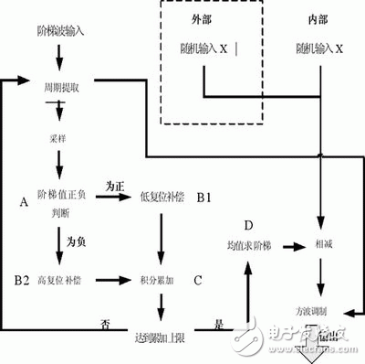
Figure 4 Software flow chart of the core algorithm of the analog header
In the flow chart, module A is used to determine the positive or negative of the step value. According to the characteristics of the actual demodulation circuit, the feedback signal is obtained by accumulating the step values ​​generated by the demodulation circuit and then being modulated by the square wave. The high and low reset operations are used in the accumulation process. Therefore, it is necessary to judge the step value positive and negative before further processing the staircase wave sample value. Here, by setting the counter, the adjacent sampling values ​​of the same period are compared for multiple times to judge the positive and negative, which avoids the influence of the sudden change of the sampling value before and after the high and low reset operation on the judgment result.
Module B is a high and low reset determination and compensation module. The module realizes the reset point judgment by comparing the sample values ​​before and after the same period, and then performs corresponding compensation operations on the reset sample values.
Functional simulation of the analog header written in Verilog HDL was performed on the Xilinx ISE8.2 platform. The Testbench module was simulated using the popular ModelSim SE 6.2 to check the correctness of the calculations and logic in the programming. The simulation module sets the main clock MCLK period to 10 ns, and the high and low levels last for the same time. Sampling is performed every 50 clock cycles, and 16 samples are accumulated to find a step. The simulation time is set to 35000ns, RSTB is the main reset signal, ADBUSY and ADCNVST are the ADC control signals, and CLOCK is the DAC control signal.
This scheme verifies the simulation results of random number X and input INDATA under several extreme conditions to detect the correctness of the header programming.
ConclusionAccording to the above software and hardware design, an analog head system capable of simulating the behavior of the fiber optic gyroscope head can be designed. During the test, the actual fiber optic gyro instrument head and modulation and demodulation circuit are interfaced with the design circuit system to obtain the desired waveform and data. Comparing the random input number of the analog header (representing the angular velocity ω) with the output of the detected modulation and demodulation circuit, the performance of the measured modulation and demodulation circuit can be effectively verified.
T Copper Tube Terminals,Non-Insulated Pin-Shaped Naked Terminal,Copper Cable Lugs Terminals,Insulated Fork Cable Spade Terminal
Taixing Longyi Terminals Co.,Ltd. , https://www.longyiterminals.com