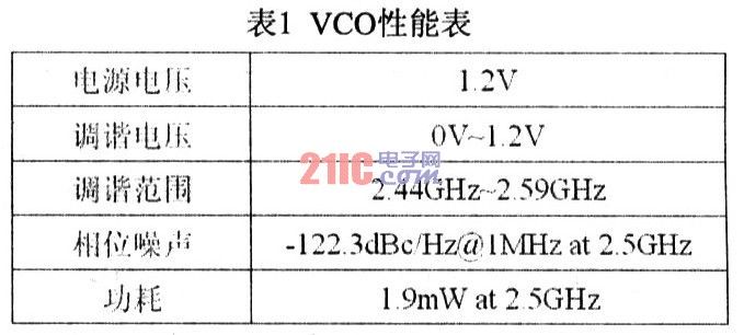
Abstract: A fully-integrated LC voltage controlled oscillator (VCO) designed with a cross-coupled structure and a TSMC90nm 1P9M 1.2V RFCMOS process conforms to the IEEE 802.1lb / g WLAN communication standard. The tuning voltage is 0 ~ 1.2V, with a tuning range of 150MHz (2.44GHz ~ 2.59GHz). Using Mentor Graphics Eldo to simulate the circuit, the simulation results show that at the 2.5GHz operating frequency, the phase noise is about -122.3dBc/Hz@1MHz, and the power consumption is only 1.9mW.
0 Introduction With the rapid expansion of the portable wireless device market, reducing system power consumption has become an important direction for RF integrated circuit design. Reducing the power supply voltage as a conventional method to reduce the power consumption of the circuit has a very obvious effect, but it must be faced with a reduction in output swing, deterioration of the signal-to-noise ratio, and the system is more sensitive to PVT (Process, Voltage, Temperature) factors, etc. Many problems.
As a key module of frequency synthesizer, voltage controlled oscillator (VCO), its stability and spectral purity are critical to the performance of communication transceiver system. How to get a better compromise between output swing, phase noise, tuning range, bias current and power consumption is the biggest difficulty of VCO design. Based on the summary of the general design method and theory of LC VCO, this paper designs a VCO suitable for IEEE 802.11b / g WLAN (Wireless Local Area Network) communication standard. In order to reduce power consumption, the VCO uses TSMC 90nm 1.2V low power supply voltage process. The simulation results show that at the center frequency of 2.5GHz, the power consumption is only 1.9mW, and the phase noise is about -122. Compared with other literatures, the same center frequency VCO design has lower power consumption and lower phase noise.
1 Basic working principle of LC VCO The cross-coupled LC VCO uses active device -g to continuously replenish the energy consumed by the LC resonant parasitic resistance g to maintain oscillation. The active device can generally be realized by the negative resistance formed by the MOS tube. In order to ensure oscillation, the conditions need to be met

Among them, αg is the gain margin coefficient, and the typical value is 2 to 3. gtank is the equivalent admittance of the LC resonant circuit, gacTIve is the negative resistance admittance, and 
The transconductance of the cross-coupled MOS tube can be expressed as 
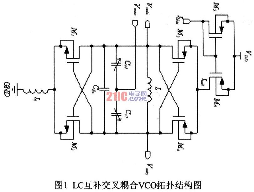
Compared with a single NMOS or PMOS cross-structure VCO, the output waveform of the complementary cross-structure VCO is more symmetrical and the noise characteristics are better. So this text chooses the VCO of the complementary cross structure, the circuit topology structure is shown as in Fig. 1. According to the basic theory of the LC oscillator, the output frequency of the VCO is 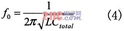
Among them, Ctotal is the total capacitance value of the VCO, including fixed capacitance Cfix, variable capacitance Cv, and parasitic capacitance Cp (inductance L, cross-coupling MOS tube and parasitic capacitance of the post-stage circuit), the tuning voltage Vtune controls Cv, and the VCO outputs The frequency factory f0 changes with the change of Vtune.
2 Circuit design
2.1 Selection of on-chip inductor L The phase noise is inversely proportional to the square of the Q value. The higher the Q value of the LC resonant circuit, the smaller the VCO phase noise. The quality factor of the on-chip capacitor is much larger than the on-chip inductance, so the quality factor of the LC resonant circuit mainly depends on the on-chip inductance. Due to the coupling capacitance between the on-chip inductor and the silicon substrate, energy will be coupled into the substrate, resulting in energy loss, thus greatly reducing the quality factor Q of the on-chip inductor. The Q value of the on-chip inductor can be obtained by measuring the Y parameter of the inductor: 
TSMC 90nm 1P9M 1.2V RFCMOS on-chip inductors are copper metal octagonal planar spiral inductors, fabricated on a P-type substrate. In order to reduce the oxide layer capacitance between the inductor and the substrate and reduce high-frequency losses, the thickest top metal in the process is usually used to make the inductor. TSMC 90nm 1P9M 1.2. The on-chip inductors in the 2VRFCMOS library use the Ultra Thick Metal process and are located on the top metal layer M9. They are divided into three types: standard (STD) inductors, symmetric inductors (SYM) and symmetric inductors with center taps. (SYMCT), adjustable parameters include inductance metal wire width w, inductance metal coil number nr and inductance inner diameter rad. In order to obtain a higher quality factor, the maximum metal line width w should be taken to reduce the parasitic resistance. Scanning simulation of S-parameters for inductors of different specifications. After calculation and comparison, the SYM inductor with dimensions of w = 15 μm, nr = 3, = 90 μm, and inductance L = 1.43nH is used. At 5GHz, its Q value is about 14.9.
2.2 Selection of negative resistance RFMOS tube RFPMOS and RFNMOS constitute a negative resistance unit for the tube, providing the energy necessary to maintain oscillation. From equations (1) to (3), W / L must be large enough to ensure vibration. When gmp = gmn, the output waveform has the best symmetry, which can effectively suppress the up-conversion of 1 / f noise. Since the mobility of electrons is 2 to 3 times that of holes, the W / L ratio of RFPMOS and RFNMOS tubes should be between 2 and 3. In order to reduce the power consumption of the oscillator and reduce the parasitic capacitance of the MOS tube, the RFNMOS tube should take the smallest size allowed by the process, that is, nr × l × w = 11 × 0.1 μm × 1 μm. Simulation results show that the output waveform has the best symmetry when the size of the RFPMOS tube is three times that of the RFNMOS tube.
2.3 Selection of fixed capacitor Cfix and variable capacitor Cv Select the MIM fixed capacitor with the parameters ff = 32.8gm, wt = 20μm and the value Cfix = 1.046pF in the library. Considering the influence of process error and external temperature, the VCO frequency tuning range should have a certain margin. After comparison, the 1.2VN well RFMOS varactor with parameters br = 8 and gr = 7 in the library is used. The simulation shows that the operating frequency of the VCO varies from 2.44 to 2.59 GHz, completely covering IEEE 802. Frequency range of b / g communication standard.
2.4 Bias current Ibias
The up-conversion noise of l / f noise has the most significant influence on the tail current source. Because the PMOS tube has lower l / f noise than NMOS, this design uses the PMOS tail current source, and the PMOS tube parameter setting is fingers × l × w = 5 × 1μm × 100μm.
The relationship between Itail and phase noise in the current limit area is as follows 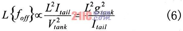
Therefore, the greater the Itail, the lower the phase noise. But if Itail increases to a certain level, it will enter the voltage limit area, and the output swing is clamped at Vlimit, which will have no meaning for the improvement of phase noise. Therefore, Itail has an optimized value corresponding to the minimum phase noise, which is located at the boundary between the current limiting region and the voltage limiting region. After considering the trade-off between power consumption and phase noise, the current source Ibias value is set to 1.8mA.
2.5 Noise filtering To further filter out the higher harmonics in the VCO output, a symmetrical inductor Lf is connected between the RFPMOS negative resistance tube and the ground terminal, and its parameter values ​​are w = 3, nr = 6, rad = 90 .
3 Simulation results Through Mentor Graphics Eldo simulation, the VCO tuning curve is shown in Figure 2. When the tuning voltage changes from 0V to 1.2V, the output frequency of the VCO increases from 2.44GHz to 2.59GHz. The phase noise characteristic curve at the center frequency of 2.5 GHz is shown in Fig. 3.

VCO performance parameters are shown in Table 1.
4 Conclusion On the basis of summarizing the general design method of VCO, this paper designs a fully integrated cross-coupled LC VCO using TSMC 90nm 1.2V RFCMOS process, which meets the requirements of IEEE 802.11b / g WLAN communication standard, which is better than other literature designs It has the advantages of simple structure, low phase noise, low voltage, and low power consumption, and is very suitable for portable WLAN transceiver equipment that requires high power saving performance.
Robust and sleek design, Ip65 Touch Screen Monitor having surface water-proof specification.
Touch speed is less than 3ms, good accuracy; supports 10 point touch.
It good to be a parts on the enclosure, serve indoor , as a IP65 Touch Screen Monitor
Aluminum alloy + sheet metal structure, nosharp edges, wear resistant and anti-corrosive paint process, overall explosion-proof design
IP65 Touch Screen Monitor has been Widely applied on the public places: subways, airports, book stores, parks, exhibition halls, stadiums, museums,convention centers
IP65 Touch Screen Monitor
Industrial Monitor,Ip65 Touch Screen Monitor,Touch Screen All In One,Touch Screen Desktop Monitor
Guangzhou TouchWo Electronics Co.,Ltd. , https://www.touchaio.com