With the development of 4G/5G mobile communication technology, the requirements for antenna-compatible multi-band are getting higher and higher. For the design, the standing wave and insertion loss of the antenna are tested. However, it is not only cumbersome to use the network to perform the plugging and unplugging. Moreover, it is easy to insert and insert multiple times, resulting in poor performance of the contact, and it is not possible to verify the correctness of the design. In this case, an automatic test method is needed to replace the manual wiring test, and the network test port is expanded (2) ), docking the antenna test port, but the design process will encounter different problems, the following step-by-step analysis
Problem phenomenon
During the test of the antenna, it was found that one of the channel standing waves and the insertion loss was abnormally large, the standing wave was 3.1 at the maximum, and the difference was 20 db. The check was due to the excessive standing wave and insertion loss of one of the ports on the PCB.
By comparison, it is found that: -45 port input, S11 port output condition test standing wave and differential loss normal, standing wave maximum is 1.53, insertion loss is maximum -7db; +45 port input, S22 output (as shown in Figure 1). The maximum standing wave is 3.2, and the maximum loss is 20db. The two circuits have the same structure. The only difference is that the length of the transmission line is different. After analysis, the standing wave value is large and the insertion loss value is large due to the circuit impedance mismatch. The next step is to solve the problem of standing wave and insertion loss.
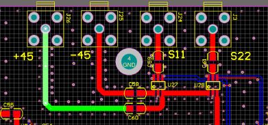
Figure 1 Test port PCB diagram
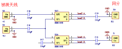
Figure 2 Test port schematic
Single port solution
1. Option 2: Change the antenna switching IC, but combined with the current performance of our antenna, only the HMC595E meets the requirements (in fact, it can be replaced by a PIN diode)
2. Option 3: Modify the design circuit to match the transmission line. Option 3 is feasible.
Multiport test
The purpose of this test is to solve the problem that the ICs interact with each other and cause the standing wave and the insertion loss to deteriorate.
Test 1: port +45 IN, port S22 OUT, other ports are left floating;
Level: U27_A is low, U27_B is high, U28_A is high, U27_B is low;
Test 2: port +45 IN, port S22 OUT, other ports are left floating;
Level: U27_A high, U27_B low, U28_A high, U27_B low;
Test 3: port -45 IN, port S11 OUT, other ports are left floating;
Level: U27_A high, U27_B low, U28_A low, U27_B high;
Test 4: Port +45 IN, port S11 OUT, other ports are left floating;
Level: U27_A is low, U27_B is high, U28_A is high, U27_B is low;
The test 2 case is to test the influence of U27 on the standing wave and insertion loss of the U28 path. From the theoretical analysis, when the U27_A level is high, the U27_B level is low, the U27_RF1 pin is not connected, the U27_RF2 pin is connected to the signal; when the U28_A is powered Flat high, U29_B level is low; U28_RF1 pin does not pass signal, U28_RF2 pin is connected signal, see Figure 4 pin diagram and truth table.
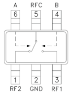
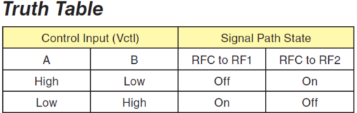
Figure 4 HMC595E pin diagram and truth table
When the signal is input from the +45 port, it passes through U28 and S22, and no signal flows through U27. However, during the test, it was found that the U27 after soldering had little effect on the input standing wave of the S22 port, and the standing wave of the S22 port was deteriorated. The maximum standing wave of the S22 port output was 1.7, and the S22 port output standing wave after the U27 was soldered. Is 2.1. As shown in Figure 5 and Figure 6.
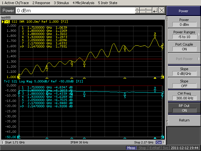
Figure 5: No-weld U27, +45 input S22 output channel standing wave and insertion loss
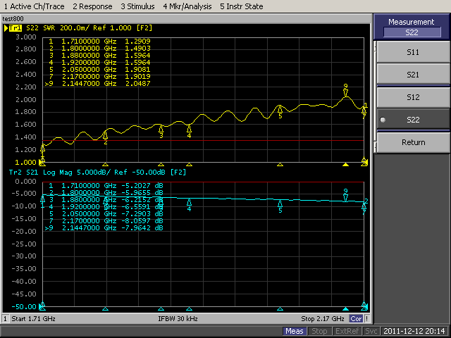
Figure 6: Welding U27, +45 input S22 output channel standing wave and insertion loss
By modifying the circuit, the impedance is matched during transmission. Through debugging, the final circuit is as follows:
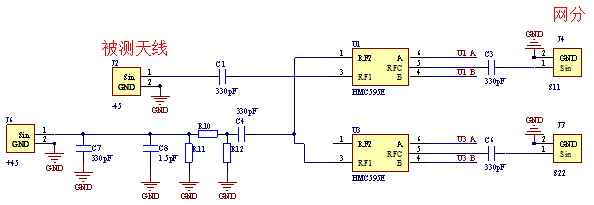
Figure 7 final debug circuit
In Figure 7, R10 = 5.1 Ω, R11 = R12 = 810 Ω, achieving 50 Ω impedance matching. The specific calculation can use the network attenuation calculation software. The software screenshot is as follows, and can also be calculated by mathematical formula. For details, please refer to the article "RF Power Attenuation Value Principle.pdf".
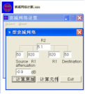
Figure 8 Network attenuation calculation software interface
The modified PCB diagram is as follows:
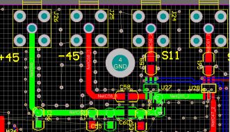
Figure 9 PCB diagram after debugging
Partial standing wave test data:
Table 1 System standing wave part test data
| Board port | antenna | system | |
| S22 | 1.54 | 1.51 | 1.78 |
| S11 | 1.55 | 1.44 | 1.58 |
Summary: This method can temporarily solve the standing wave and insertion loss problem, but can not accurately determine the parameters of the circuit and the parameters of the PCB layout, which is not conducive to improving work efficiency. In the next article we will study the essential causes of the problem.
USB C HUB,6 in 1 Type C Hub with Ethernet, 6 in 1 USB-C hub to HDMI,USB-C 6-in-1 Multiport Adapter,6 in 1 Multiport USB-C,USB-C Adapter Docking Hub
Shenzhen Konchang Electronic Technology Co.,Ltd , https://www.konchangs.com