Introduces a 2.4 GHz low noise sub-sampled phase-locked loop. Loop lock is the sampling of the output of the voltage controlled oscillator using a subsampling phase detector. Unlike the traditional charge pump phase-locked loop, the in-band noise generated by the phase detector and the charge pump is not amplified by N2 times due to the absence of the divider in the locked state, thus making the phase-locked loop in-band. The noise is greatly reduced. In the case of the same output voltage swing, the voltage controlled oscillator uses the NMOS-PMOS complementary structure to reduce the power consumption of the phase-locked loop. The phase-locked loop is designed in a TSMC 180 nm CMOS process with a phase-locked loop power dissipation of 7.2 mW at a supply voltage of 1.8 V. At an offset carrier frequency of 200 kHz, the in-band noise of the loop is -124 dBc/Hz.
introductionIn wireless communication systems, a low jitter, low noise clock signal is essential. Phase-locked loops are currently widely used to generate high-precision clock signals, such as providing a stable local oscillator clock signal for a wireless RF transceiver system. The low noise local oscillator signal plays a vital role in the overall performance of the wireless transceiver system.
In the conventional charge pump phase-locked loop, the in-band noise performance is greatly deteriorated due to the action of the frequency divider. Typically, a smaller loop bandwidth is chosen to suppress the in-band noise caused by the phase frequency detector and the charge pump. However, reducing the loop bandwidth increases the lock-in time of the phase-locked loop and the chip area.
Since the sub-sampled phase-locked loop has no frequency divider function in the locked state [1], the compromise between loop bandwidth and noise can be well solved, and a large loop bandwidth can be obtained and reduced. Phase noise of the small phase-locked loop.
In this paper, the in-band noise of the traditional charge pump phase-locked loop is analyzed. A low-noise sub-sampled phase-locked loop is proposed. The specific implementation and circuit simulation results of each module are given.
1 In-band noise of conventional charge pump phase-locked loopFigure 1 shows the basic structure of a conventional charge pump phase-locked loop (CPPLL) [2], mainly consisting of Phase and Frequency Detector (PFD), charge pump (CP), and loop filter (Low Pass Filter, LPF) and voltage controlled oscillator (VCO). Figure 2 shows the phase noise model of CPPLL [3], Kd is the PFD/CP linear gain, FLPF(s) is the transfer function of the loop filter, and KVCO/s is the gain of the VCO.
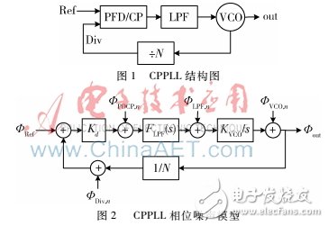
The CPPLL in-band noise is mainly contributed by the noise of PFD/CP. Using the phase domain model of Figure 2, the noise transfer function of the closed-loop PD/CP can be obtained as follows:
HPDCP(s)=φout,nφPDCP,n=1Kd·G(s)1+G(s)/N(1)
Among them, G(s)=Kd·FLPF·KVCO/s is the PLL open-loop transfer function. Therefore, the in-band noise contributed by PFD/CP is:
Where Kd=ICP/2Ï€, phase noise Linband is usually expressed as single sideband noise power, and SiPDCP is PFD/CP noise frequency spectral density. It can be seen from equation (2) that the in-band noise of the PLL is amplified N2 times due to the existence of the frequency divider. Therefore, a larger Kd, CP, that is, a larger PFD/CP linear gain Kd and a smaller frequency division ratio N will result in better noise performance.
2SSPLL working principle and noise analysisThe basic block diagram of the sub-sampled phase-locked loop proposed in this paper is shown in Figure 3. It is mainly composed of the core sub-sequence loop (Core Loop) and the frequency-locked loop (FLL). If only the core circuit is used, since the SSPD has a limited capture range, the sampler cannot distinguish whether the sampled frequency is the required N·fRef or other harmonics of fRef during the sampling process. Therefore, adding the FLL can obtain the required lock. frequency. The SSPD samples the output of the VCO with a reference signal Ref. Using the same SSPD/CP as the Dummy sampler eliminates the charge injection from the sampling switch to the VCO and compensates for the BFSK effect [4], thereby optimizing the reference spur performance of the sampling PLL.
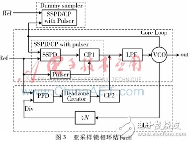
When the loop is not locked, the core sampling circuit works with the FLL. When the phase difference between the DF and the FLL divider output Div is less than π, the output of the PFD will fall into the dead zone, so that the CP2 cannot be turned on and the FLL stops working. Only the core sampling circuit works alone until it is locked. When the loop is locked, the rising edge of Ref is aligned with the intersection of the VCO differential output waveform. After the SSPD is sampled, the sampled voltage can be converted to the upper and lower currents IUP and IDN by the CP. Since the voltages obtained by Ref sampling are equal, the upper and lower currents of the CP are equal, so that the VCO control voltage VCTRL remains constant and the loop is locked.
Since the FLL does not work when the loop is locked, the noise model of the SSPLL can be simplified to the model shown in Figure 4. Compared with Figure 2, it is obvious that the influence of the frequency divider module on the system is reduced, so that the in-band noise of the phase-locked loop is greatly reduced. Thus the noise contributed by SSPD/CP to the entire loop is:
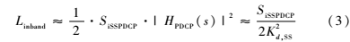
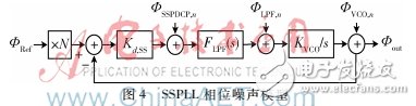
However, the noise of the reference source is still amplified by N2, so in SSPLL, the in-band noise is mainly contributed by the noise of the reference source.
3 circuit design and implementation of each module 3.1 voltage controlled oscillator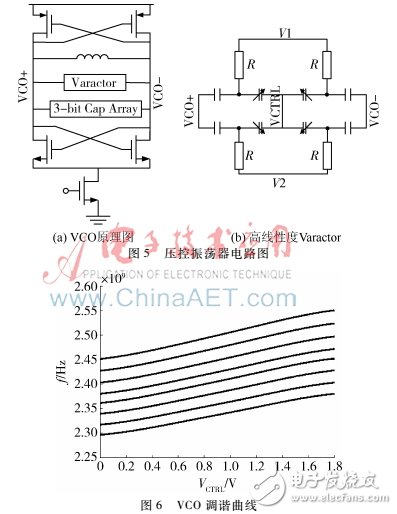
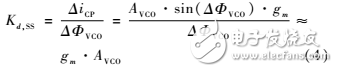
Figure 5 is a voltage-controlled oscillation circuit diagram, (a) is a schematic diagram of the VCO, this paper is designed to use NMOS-PMOS complementary structure. Compared to a full NMOS, full PMOS structure, this structure not only saves power, but also provides better phase noise when the bias current is equal [5]. In addition, when the bias current is constant, the complementary structure provides a larger negative resistance value, and the cross-coupling tube has a faster switching speed, so that the corner frequency of the 1/f noise is greatly reduced. At a bias current of 1 mA, the phase noise can reach -120 dBc/Hz @ 1 MHz. (b) For the high linearity Varactor, the symmetrical structure of the VCO varactor Varactor can effectively improve the linearity of the frequency tuning gain KVCO to optimize the noise performance. The design of KVCO is 55 MHz/V, the tuning range is 2.3 GHz~2.55 GHz, and the tuning curve is shown in Figure 6.
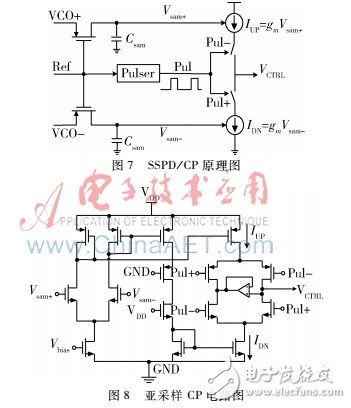
3.2 Subsampling Phase Detector / Charge PumpFigure 7 shows the schematic diagram of the SSPD/CP. Figure 8 shows the circuit diagram of the sub-sampled CP proposed in this paper. During the sampling process, the ideal sampling point is the zero-crossing point of the sinusoidal signal when locking, so that:
Comparing the noise performance of the sub-sampled phase-locked loop CP with the traditional charge pump phase-locked loop CP, you can get:
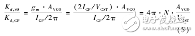
Normally, N 1, AVCO / VGST "1, so Kd, SS-Kd, CP. Comparing equations (2) and (3), the in-band noise of the sub-sampled phase-locked loop can be greatly suppressed. However, in the case where the loop bandwidth is constant, the CP gain is excessively large, resulting in an excessive capacitance of the loop filter, so that the area of ​​the chip is increased. The pulse generator Pussel circuit is added to control the CP conduction time, effectively control the CP gain, and reduce the chip area.
In addition, a unity gain buffer is added to the sub-sampled CP. When the output charge-discharge switch is turned off, the drain-side voltage of the current source tube is the same as the control voltage, which effectively reduces the current ripple caused by charge sharing and improves the sub-sampling. Sampling the spurious performance of the phase-locked loop.
4 circuit simulation results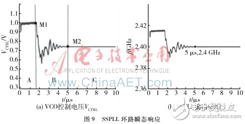
Figure 9 shows the SSPLL loop transient response. It can be seen that the output frequency of the SSPLL varies with the VCO control voltage. The A region in Figure (a) indicates that the system detects that the phase difference between Ref and Div is less than π, but the frequency is at other harmonics of Ref and is not locked. At this time, the FLL does not work, the CP2 output is 0, only the SSPD/CP has a current output, the SSPLL output frequency is greater than the required lock frequency, and the phase difference between Ref and Div gradually increases; the B region represents the phase difference between Ref and Div at M1. Accumulated to greater than π, CP2 is turned on, the loop filter discharge causes the VCTRL voltage to decrease, so that the SSPLL output frequency is reduced to be close to the lock frequency N·fRef; at M2 in the C region, the loop begins to lock, the VCO controls the voltage and The SSPLL output frequency remains unchanged.
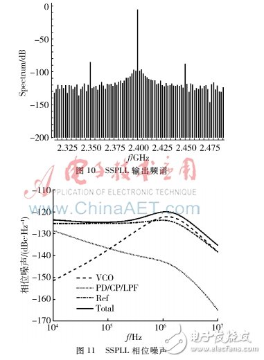
Figure 10 and Figure 11 show the output spectrum (Spectrum) and phase noise performance of the SSPLL, respectively. As can be seen from the figure, the reference spur of the SSPLL is -79.81 dBc, and the in-band noise is -124 dBc/Hz at an offset carrier frequency of 200 kHz. The layout of the SSPLL is shown in Figure 12. The core circuit area is 750 μm × 560 μm.
This paper introduces the working principle of the sub-sampling phase-locked loop circuit, and focuses on the noise performance of the sub-sampled phase-locked loop and the traditional charge pump phase-locked loop. Based on the TSMC 180 nm process, the SSPLL consumes 7.2 mW at a supply voltage of 1.8 V; the in-band noise is -124 dBc/Hz at an offset carrier frequency of 200 kHz; the reference spur is -79.81 dBc.
Laptop AC adapter for common brands, such as HP, Sony, Lenovo, Dell, Asus, Toshiba, Acer, Samsung etc. Our products have high quality and reasonable price.
CE, FCC, ROHS certification are approved by our products, and it have two years warranty. Built with input/output overvoltage protection, input/output overcurrent protection, over temperature protection, over power protection and short circuit protection. We are a professional power adapter manufacturer in China. We can meet your specific requirement. We have perfect after-sale service and technical support.
Hope we can establish friendly business relationship with you in the near future!
Laptop Adapter,Adapter For Macbook,Power Supply For Macbook, Charger For Macbook
Shenzhen Waweis Technology Co., Ltd. , https://www.waweis.com