With the advent of the information age, the use of PCB boards is becoming more and more extensive, and the development of PCB boards is becoming more and more complicated. As electronic components are more and more densely arranged on the PCB, electrical interference has become an inevitable problem. In the design and application of multi-layer boards, the signal layer and the power layer must be separated, so the design and arrangement of the stack is particularly important. A good design scheme can greatly reduce the effects of EMI and crosstalk in the multilayer board.
In the design of the multi-layer board than the ordinary single-layer board, a signal layer, a wiring layer, and an independent power layer and a ground layer are arranged. The advantages of the multi-layer board are mainly reflected in providing a stable voltage for digital signal conversion, uniformly adding power to each component at the same time, effectively reducing interference between signals.
The large area of ​​copper power supply and the ground layer can greatly reduce the resistance of the power layer and the ground layer, make the voltage on the power layer stable, can ensure the characteristics of each signal line, and are very beneficial to impedance and to reduce crosstalk. In the design of high-end circuit boards, it has been clearly specified that more than 60% of the stacking scheme should be used. Multilayer onboard, electrical characteristics, and suppression of electromagnetic radiation have unparalleled advantages over low-level boards. In terms of cost, in general, the more the number of layers, the more expensive the price, because the cost of the PCB board is related to the number of layers, and the density of the unit area appears. After reducing the number of layers, the wiring space will be reduced, thereby increasing the wiring density , Even to reduce the line width to say the short message distance to meet the design requirements. These may increase costs appropriately. It may reduce stacking and reduce costs, but it will make electrical performance worse. This design will usually be counterproductive.
Looking at the PCB microstrip wiring on the model, the ground plane can also be regarded as a part of the transmission line. The ground copper layer can be used as a return path for signal lines. The power plane is connected to the ground plane through decoupling capacitors under AC conditions. The two are equivalent. The difference between low-frequency and high-frequency current loops lies in. At low frequencies, the current flows back along the path of least resistance. At high frequencies, the current flows back along the loop with the smallest inductance. The current backflow is concentrated and distributed directly under the signal trace.
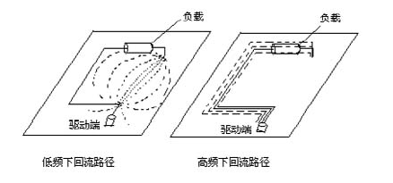
In the case of high frequencies, if a wire is placed directly on the ground layer, even if there are more loops, the current will flow back from the wiring layer under the originating path back to the signal source. Because this path has the smallest impedance. This use of large capacitive coupling to suppress the electric field, and the minimum capacitive coupling to suppress the magnetic plant to maintain low reactance, we call it self-shielding
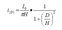
It can be seen from this formula that when the current flows back, the distance from the signal line is inversely proportional to the current density. In this way, the loop area is minimum and the inductance is minimum. At the same time, it can be concluded that if the distance between the signal line and the loop is close, the currents of the two are similar and the directions are opposite. And the magnetic field generated by the external space can be cancelled, so the external EMI is also very small. In the stack design, it is best to allow each signal trace to have a very close ground plane.
In the crosstalk problem of the ground plane, the crosstalk caused by the high-frequency circuit is mainly inductive coupling. It can be derived from the above current loop formula that the loop current generated by the two signal lines closer together will overlap. Therefore, magnetic field interference will occur.

In the formula, K is related to the signal rise time and the length of the interference signal line. In the stacked arrangement, shortening the distance between the signal layer and the ground layer will effectively reduce the interference from the ground layer. When the power layer and the ground layer are laid on the PCB wiring, a separation wall will appear in the copper area. The occurrence of this kind of problem is most likely due to the high via density or the unreasonable design of the via isolation area. This slows the rise time and increases the loop area. The inductance increases and crosstalk and EMI are generated.
When we shop, we should try to set up pairs of shops. This is to consider the requirements of the balance structure in the process, because the unbalanced common may cause the deformation of the PCB board. For each signal layer, it is best to have an ordinary city as the interval. The distance between the high-end power supply and the copper city is conducive to stabilizing and reducing EMI. In the design of high-speed boards, additional ground layers can be added to isolate the signal layer.
Hybrid Three Phase Solar Inverter
Shenzhen Jiesai Electric Co.,Ltd , https://www.gootuenergy.com