Wang Wei, Jiang Jinghong, Liu Hao, Cai Huizhi, Institute of Acoustics, Chinese Academy of Sciences
Keywords: COM Express; PCI Express bus; recorder; fiber data acquisition
In the field of military applications, processing platforms based on general-purpose signals usually require high-speed and large-capacity data storage. How to solve data I/O and memory bandwidth bottlenecks to meet the requirements of radar and sonar systems for high-speed and large-capacity data storage, and how to develop common and open storage modules based on different architecture platforms is a problem that needs to be solved. .
At the present stage, a data recorder for sonar adopts the CPCI architecture. The communication interface between the data acquisition board and the signal processor in the recorder adopts parallel LVDS cable. The data acquisition board submits the received data through the PCI bus. Store to the main control board. Due to the double limitations of crosstalk between parallel cables and PCI bus bandwidth, the performance, versatility, and scalability of the recorder are poor, and the storage rate is not ideal, which does not meet the requirements of future sonar systems for real-time data storage. Therefore, research on data loggers based on new architectures and high-speed serial buses has become very urgent.
Based on the above problems, this paper presents a new data recorder based on COM Express architecture design and implementation methods, and its hardware components - the fiber collection daughter card was discussed in detail, and finally gave the test results.
1 Recorder System Structure and Key Technologies
1.1 Recorder System Structure
This design considers the architecture system and the bus structure. The ETXexpress-PC module of the German Kontron Corporation is selected as the processor unit. The XMC-PCIE mezzanine card is designed as the fiber data acquisition module on the COM Express carrier board. At the same time, the use of four 500 GB disks to form a RAID0 storage array completes the design of the new logger. Recorder structure diagram shown in Figure 1.
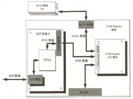
Figure 1 Recorder block diagram
Kontron's ETXexpress-PC module uses Intel's 45nm process-level Core 2 Duo processor and GS45 and ICH9M chipsets to support high-speed interfaces such as SATA, USB, PCI Express, and Gigabit Ethernet, and the modules are strictly compliant with COM. The Express specification facilitates the upgrade of the carrier board and reduces the waste of resources caused by repetitive design.
To speed up product development, the recorder is designed primarily on the basis of a COM Express evaluation board provided by Kontron. In a limited space on the carrier board, in order to provide sufficient space for the installation of the fiber capture card, the peripheral interface necessary for the original carrier board, such as VGA, PS/2, RS232, USB, and LAN, is reserved, and the Express Card, Mini Express are removed. Loggers do not require interfaces that take up a lot of space. There is no space for the hard disk on the carrier board because the hard disk is designed for the convenience of hard disk removal and replacement in actual applications. The SATA hard disk is connected to the carrier board through a customized hardened SATA cable, so you only need to install a custom SATA card connector in the appropriate position on the carrier board.
1.2 Key technologies
COM (Computer On Module) Express is a computer module standard defined by the International PICMG Association and is jointly developed by several large embedded industrial computer manufacturers. The COM Express processor module integrates the CPU and North and South Bridge chips. All I/O functions are implemented using two 440-pin two-row Connectors AB and CD. Among them, the AB connector defines high-speed interfaces such as PCI Express, SATA, SDVO, Gigabit Ethernet, and USB. The CD connector defines traditional parallel bus interfaces such as PCI and IDE. The user can select processor modules with different CPU performance, power consumption, and I/O capabilities according to different application scenarios, and develop different functional modules. Functional modules are generally designed as standard interfaces that are connected to the carrier via specific connectors. Compared with the traditional CPCI architecture, COM Express has the advantages of rich interfaces, flexible use, and short development cycle.
Digital optical fiber communication is a kind of long-distance data transmission technology, which has the advantages of high bandwidth, low delay, high reliability, long transmission distance, strong anti-interference, and mature technology. The point-to-point optical fiber communication rate can reach 2 Gb/s to 4 GB/s, which has a wide application prospect in the field of remote data acquisition and remote real-time monitoring. This design uses optical fiber instead of parallel LVDS cable as the data acquisition interface of the recorder to overcome the problems of high-speed crosstalk and communication distance.
The theoretical transmission rate of the traditional 32-bit/33-MHz PCI bus is 133 MB/s, which is far from the requirement and has become the main factor that restricts the storage performance of the recorder. PCI Express is the third generation of high-performance I/O bus. It has changed from a parallel bus to a serial bus on the bus structure. It uses point-to-point interconnection to greatly increase the transmission bandwidth of the system. And its bus structure maintains compatibility with the PCI bus from the address space, configuration mechanisms, and software. The use of a PCIE bus instead of the PCI bus as a data path between the data acquisition card and the main control board not only drastically improves the performance of the storage but also maintains good upward compatibility.
Disk array (RAID) refers to the use of multiple hard disks combined by a RAID controller (software or hardware controller) into a virtual single large-capacity hard disk, providing various quality of service through resource redundancy. For example, organizing multiple independent disks into one logical disk provides greater storage capacity; improves data I/O rates through data partitioning and multi-channel parallelism; improves storage by storing redundant data and verifying information System reliability and so on. The use of multi-disk RAID technology will greatly increase storage capacity, storage speed, and reliability.
2 Design of Fiber Acquisition Card
2.1 Fiber Acquisition Cards Overview
The fiber capture card is the core of the recorder. The board is developed based on Xilinx's Virtex5 series FPGA chip XC5VLX50T. It conforms to the size, shape and mechanical structure defined in the VITA 42.3 XMC PCI Express specification and uses Samtec's standard XMC connector ASP-105885 and COM Express. Interconnect communication between boards. The board consists of a fiber interface module, a DDR2 cache module, a PCIE interface module, a power management module, a clock management module, and a reset circuit. The system block diagram is shown in FIG. 2 .

Figure 2 Optical Fiber Acquisition System Block Diagram
2.2 Fiber Interface Design
The fiber-optic module uses FTISAR's FTLF1321 SFP high-speed transceiver. The work flow of optical fiber collection is: the optical transceiver receives data and performs photoelectric conversion, and then transmits the serial data to the Rocket IO hard core of the FPGA for serial-to-parallel conversion, and finally stores the parallel data in the internal FIFO of the FPGA. In order to increase the reliability of data, reduce the bit error rate, and match the rate of sending and receiving dual transmissions, flow control, data management, and encoding and decoding mechanisms must be introduced. Therefore, the Aurora protocol provided by Xilinx is used to drive the Fibre Channel. And management. The Aurora protocol is a compact, lightweight, and tailorable communication protocol that is very flexible, uses less system resources, and can expand multiple Fibre Channel channels.
2.3 DDR2 Cache Design
Since the data acquisition systems are real-time systems, the collected data is continuously sent to the recorder. The non-real-time nature of the Windows operating system, kernel scheduling, and unpredictability of multi-threaded operations may cause data loss. Therefore, in order to ensure the reliability of the recorder and reduce the buffer pressure of the processor module, a buffer device with large capacity and fast access capability should be designed on the fiber acquisition card. The board chose two Micron MT47H128M16B DDR2 SDRAMs for caching. The chip uses a 1.8 V core voltage and supports up to 667 MHz clock frequency. This design uses Xilinx's memory management generator IP core MIG3.1 to develop DDR2 controllers and complete FPGA control of DDR2. While managing the data cache, the DDR2 controller also needs to manage the DMA transfer interrupt request with the PCIE bus control module.
2.4 PCIE bus control logic design
PCIE bus control logic is a difficult point for optical fiber acquisition cards. Because the PCIE endpoint block is embedded in the XC5VLX50T device, the IP core implements the full functionality of the PCIE bus. Therefore, the PCIE endpoint block hardware and the Rocket IO hard core of the FPGA can be used to implement the physical layer and link of the PCIE protocol. Layer and transport layer functions. The interaction between the PCIE bus and the processor can be done either through PIO or DMA. The PCIE hard core itself only contains the functional modules of the PIO, and the PIO mode requires the participation of the CPU, and thus affects the operating efficiency of the CPU. In order to meet the real-time and high-speed storage of data, a DMA controller has been designed to complete the DMA function. The PCIE protocol specifies that PCIE transactions can be divided into four types: memory transactions, IO transactions, configuration transactions, and message transactions. The execution or completion of the transaction is specifically implemented by sending and receiving transaction packets (TLPs), that is, communication between the PCIE endpoints and the CPU through the TLP. The TLPs that need to be used in this design mainly include memory read TLP (MRd), memory write request TLP (MWr), and data completion TLP (CplD). Therefore, the PCIE bus control logic focuses on the construction and analysis of PCIE transaction packets, the management of interrupts, and the control of DMA transfers. DMA control logic diagram shown in Figure 3.

Figure 3 DMA control logic diagram
The main module functions in Figure 3 are as follows:
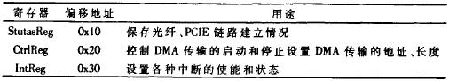
(1) The DMA status/control register module is mainly responsible for the management of board status, management of DMA transfers, and partial management of interrupt signals. When instantiating the PCIE endpoint block hardware, the system requests the BAR0 memory space of 128 B to store these registers. The main registers are shown in Table 1. After the board driver is loaded, the CPU reads the StutasReg register to check the status of the kanban card. If the fiber link or the PCIE link fails, the module is responsible for giving the corresponding fault indication signal. If the board status is normal, the CPU writes the DMA transfer address and length information to the CtrlReg register and writes the corresponding interrupt enable flag to the IntReg register.
(2) The data transmitter module is responsible for reading data from the data preparation module, constructing MRd, MWr, CplD transaction packets, and sending them to the endpoint block. The data prepared by the data preparation module comes from the transmit FIFO or DMA status/control register.
(3) The data receiving module is responsible for receiving and parsing the MRd, MWr, CplD transaction packets from the endpoint block, storing the received data in the receiving FIFO, DMA status/control registers, or notifying the data transmitter module to construct the corresponding CplD transaction packet.
(4) The interrupt management module is responsible for interrupt signal generation, clearing, and reset. It mainly manages four types of interrupts: DMA read interrupt request, DMA read completion interrupt request, DMA write interrupt request, and DMA write completion interrupt request. Among them, the DMA interrupt read/write request is given by the DDR2 controller. It is used to inform the CPU optical capture card that the buffer space/cache data amount is enough to achieve a read/write DMA transfer length; the DMA read/write completion interrupt is controlled by The interrupt management module gives notification to the CPU that the read/write DMA transfer has been completed.
The flow of a write DMA data transfer is as follows: (1) The DDR2 cache module buffers the data received by the optical fiber, and sends a DMA write interrupt request to the interrupt management module when the buffered data amount reaches a set threshold. The interrupt management module passes this interrupt to the endpoint block, interrupts the CPU via the PCIE link, and writes the IntReg register to record the type of this interrupt. (2) After the CPU receives the interrupt, it initiates a memory read transaction and reads the corresponding bit in the IntReg register. After it is determined that the DMA writes an interrupt request, a memory write transaction is initiated to the CtrlReg register to initiate the DMA transfer. At the same time, the CPU initiates a memory write transaction to the IntReg register to disable the DMA write interrupt and open the DMA to complete the write interrupt. (3) After the DMA is started, the CPU does not need to participate in the data transfer, and the rest of the transfer work is done by the DMA controller. The write DMA transfer of data is essentially the DMA control logic continuously writing TLP to the DMA buffer driven by the board. Each time a TLP is sent, the DMA transfer length value is subtracted from the last TLP data length and is reduced to zero. (4) When the DMA transfer ends, the interrupt manager will send a DMA write completion interrupt to the CPU and write the IntReg register again to record the type of this interrupt. (5) After the CPU receives and judges this interrupt, it will notify the application program to read the received data and save it. At the same time, it will open the DMA write interrupt, close the DMA write completion interrupt, and wait for the next write DMA transfer.
3 system debugging and performance testing
A logger storage test platform was set up to verify that the DMA transfer of the system was designed in accordance with the timing specified by Xilinx's PCI Express endpoint block IP core and the performance of SATA storage. The platform is sent by the signal processor through the optical fiber to the recorder for data stored in 32-bit increments. The hardware logic of the FPGA is implemented under the Xilinx integrated development environment ISE 11.2, so the PHY transfer timing diagram shown in Figure 4 can be captured using the online logic analyzer ChipScope.
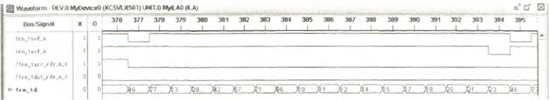
Figure 4 PCIE timing diagram
It can be seen from Figure 4 that between the two low levels of trn_sof_n and trn_eof_n is a TLP transmitted by the PCIE bus, which fully complies with the timing requirements of the endpoint block IP core and verifies the logical design of the DMA.
After the data is transferred from the acquisition card DMA to the driver buffer, the application completes the data extraction from the driver and writes the disk. Lastly, the read-verification of the stored data is verified by the Matlab program, which verifies the correctness of the data recorded by the recorder. Table 2 shows the effect of the average save rate on different single DMA lengths and single save lengths.
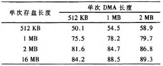
From Table 2, it can be seen that the storage rate of the recorder is greatly affected by the data length of a single save, and is relatively small due to the single DMA length. The reasons are: (1) The data transfer rate of PCIE is much greater than the data save rate; (2) The software overhead of non-real-time operating systems is large. The more times the data of the same size is manipulated, the more time it takes. long. Therefore, you should try to increase the data length of a single save to increase the storage performance of the recorder.
This paper implements a design of a new recorder based on the COM Express architecture. This design mainly completes the high-speed acquisition of fiber data, DMA transfer between the processor modules, and high-speed storage of data. The practical application shows that the recorder is greatly improved in terms of stability and storage rate compared with traditional recorders, and can be well qualified for future acquisition and storage of sonar data. Moreover, because COM Express is an open architecture, it provides many mainstream high-speed interfaces that can flexibly extend other functional modules and provide a new idea for embedded design.
Connectors
We have experience and skill to support customers to tooling for their required waterproof connectors, like IP68 series,micro fit connectors. Etop wire assemblies for various industries have been highly recognized by all the customers and widely used for automobiles, electrical and mechanical, medical industry and electrical equipemnts, etc. Products like, wire harness for car audio, power seat, rear-view mirror, POS ATM, Diesel valve Cover gasket fit, elevator, game machine, medical equipment, computer, etc.
JST Connector,Molex Connector, Multi-Contact Connector, Micro Fit Connectors
ETOP WIREHARNESS LIMITED , http://www.oemwireharness.com