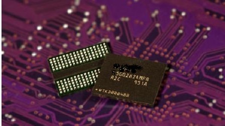
 After the NAND Flash memory enters the processing node below 20nm, it will face severe challenges of micro-miniature, so memory manufacturers have stepped up to invest in new technology research and development, with a three-dimensional (3D) space storage lattice structure or charge trap (Charge Trap). Technology, to realize a new generation of NAND Flash products with small size, high capacity, high stability and taking into account development costs.
 Non-volatile memory applications can be divided into independent and embedded system solutions. Stand-alone applications are driven primarily by the continuing demand for costs and next-generation products. Although the cost of embedded solutions is important, long product life, extended performance (such as extended temperature range, higher reliability, lower power consumption, etc.) and support capabilities are also key considerations for embedded systems. The embedded market mainly relies on the high reliability and performance of NOR Flash for important applications such as code storage, while NAND is usually used for less important data storage.
Floating gate NAND faces restrictions In recent years, compared to NOR, NAND technology has been more active in reducing the size, but it also faces greater challenges. Therefore, the industry is evaluating some forward-looking technologies with the goal of achieving scalable, higher capacity and reducing costs with acceptable levels of performance and reliability.
Although the industry has found a feasible way to expand NAND, it is still challenging to use floating gate technology that exceeds 20 nanometers (nm) to maintain the development of the previous industry. The main challenge of the extended floating gate technology is the continuous reduction of the spacing between the cell grids, the difficulty of implanting the necessary interlayer dielectrics and the control gates between adjacent cell grids for the smaller gaps. Not only that, the shorter cell spacing also greatly increases the capacitance. Coupling causes interference with adjacent cells.
20 nanometers technology charge extraction and 3D NAND head struggle To continue to expand the NAND Flash market, the industry is evaluating two possible ways to expand the following 20 nanometer technology - three-dimensional (3D) space cells or planar cells, such as charge Capture (CT) NAND technology.
The 3D Flash technology uses a stacking method. The so-called technical layer stacking, like each floor of a high-rise building represents a different memory cell. The challenge with this technology is that the product will have a very high "stacking" with a high aspect ratio (height exceeds the width), creating process challenges for Uniform Patterning and Depositing Material. In addition, high aspect ratio stacked cell structures also contribute to structural instability.
The difference between planar charge extraction NAND technology and traditional floating gate technology is that it uses an ultra-thin GaN layer of about 100 angstroms (Angstrom) to store electrons, rather than a conventional floating gate storage layer of more than 1,000 angstroms. The thinner tantalum nitride film layer greatly reduces the capacitive coupling of adjacent cells and also eliminates the challenge of implanting a sandwich dielectric between narrow and high aspect ratio floating gates.
Resistive RAM
Some companies, universities and national laboratories are exploring another new non-volatile technology - Resistive Random Access Memory (RRAM) (Figure 2). The RRAM defines the 0 and 1 states of the memory by changing the electrical properties of the dielectric material between the two metal contact layers to form the properties of two different resistors.
A key issue in RRAM research is to find the right combination of materials. Bridge-based and Oxygen-based conductivity are currently more forward-thinking materials.
The bridge-based conductive RRAM is composed of two metal contact layers (including one layer of silver), with a high-resistance insulator interposed therebetween, and a voltage-introduced metal layer to form a silver-based conductive filament, resulting in a low-impedance state. When the voltage direction is changed, the conductive wire between the metal contact layers is disconnected to form a high impedance state, which is the two states of the memory. The biggest challenge with bridge-based conductive RAM is the ability to create repeatable, reconstructable filaments in many single and multiple cells in memory. Another important point to note is that because bridge-based conductive RRAMs often rely on materials (such as silver) rather than the usual crucible production equipment, they will face the challenge of pollution and process when introducing these new materials into the foundries.
Oxygen RRAM uses an oxide insulator between two metal contact layers. The selection and engineering of the oxide material is non-stoichiometric (it can make the oxygen level too high or too low). When the voltage is applied to the contact layer of the metal, it can be controlled according to the direction of the bias voltage so as to generate a high or low resistance when passing through the insulator path. Similarly, the biggest challenge with oxy-RRAM is also to create repeatable, reconstructable paths in many cells and multi-layer cells. Oxygen materials (such as yttrium oxide) are currently more in line with existing bridge-fabric equipment specifications than bridge-based conductive materials.
To make RRAM a competitive solution requires good manufacturing equipment. At present, the industry is trying to use diodes in the metal layer instead of transistors in the germanium base, because this geometric space is small enough to actually be used to build the next generation of non-volatile storage.
The phase change memory (Phase Change Memory) also consists of two metal contact layers. The middle two metal contact layers are a chalcogenide material, mostly based on a germanium-based sulfide system (GeTeSb), which can be either an amorphous insulating phase or a polycrystalline germanium conducting phase.
These materials undergo phase transitions through heating and quenching. It is heated locally through the material via a flowing current, which is accomplished at a high temperature of 600 degrees. In the past 1-2 years, several companies have introduced low-capacity phase-change random access memory (PCRAM) into the market. However, the number of PCRAM programming cycles is limited, the programming time is slow, and the performance at high temperatures is poor. PCRAM also requires high current and high power to reach the temperature required for programming, and it is difficult to scale up.
Magnetoresistive Random Access Memory Many companies, universities and research laboratories are currently exploring magnetoresistive random access memory (MRAM). The MRAM has magnetization switching (Toggle) and spin torque (Spin-torque) versions.
MRAM is composed of two metal contact layers. The metal contact layer in between has two layers of magnetic material separated by an insulator, one of which is fixed in the direction of polarization and the other is switchable. If two magnetic materials have the same polarization direction, the memory cell is in a low-resistance state. Conversely, if the two have opposite polarization directions, the memory is in a high-impedance state.
When the magnetized MRAM program is switched, current will be introduced into the metal wire braided on top of the magnetic material to generate a local magnetic field. The sequence of currents applied between the two wires determines one of the polarization directions of the magnetic layers in a direction relative to the other.
When rotating torque is programmed in the MRAM program, the current actually flows through the entire material stack. Most electrons in a fixed magnetic layer rotate in the same direction. According to the direction in which the current passes through the fixed magnetic material, the electrons in the fixed magnetic layer interact with the electrons in other magnetic layers, forcing the stationary magnetic layer electrons to spin in the opposite or the same direction.
Switching Magnetized MRAM's current mass production capacity from 256Kb to 16Mb. Switching magnetized MRAMs have fast read/write access times and infinite read/write cycles. Expanding the ability to switch magnetized MRAMs to smaller geometries and larger capacities is highly challenging. As for another solution, the rotational torque MRAM is expected to have high expandability and a small switching current. However, the rotating torque MRAM is still in the research phase. The challenge with rotating torque MRAM is how to achieve reproducible, repeatable exchange while maintaining reliability requirements.
MRAM, PCRAM, and RRAM are becoming major memory technologies and will be highly dependent on new material innovations. On the other hand, planar charge extraction NAND and 3D NAND can utilize existing materials and quickly become a viable replacement for high-capacity floating gate NAND.
Ceramic Line Post Insulator are a type of steel insulator, Line Post Insulator is used for supporting wires and resisting electric current, High Voltage Line Post Insulation consisting of one or more insulating members permanently glued to a metal base, sometimes with a cap,and can be double mounted on a metal base. The head bolt or one or several bolts are steel mounted on the support structure. Porcelain Power Line Insulators are suitable for temperatures between -40° C to +40° C, heights below 1000m(1000m and above can be amend base on GB311.1-1997), frequencies not exceeding 100Hz, voltages above 1000V, and mechanical loads within the rated values of the product.
| MAIN DIMENSIONS AND STANDARD PARTICULARS | |||||
| ANSI Class | 57-1 | 57-2 | 57-3 | 57-4 | 57-5 |
| Creepage Distance/mm | 356 | 559 | 737 | 1015 | 1145 |
| Dry Arcing Distance/mm | 165 | 241 | 311 | 368 | 438 |
| Cantilever Strength/kn | 12.5 | 12.5 | 12.5 | 12.5 | 12.5 |
| Low Frequency Dry Flashover Voltage/kv | 80 | 110 | 125 | 150 | 175 |
| Low Frequency Wet Flashover Voltage/kv | 60 | 85 | 100 | 125 | 150 |
| Critical Impulse Flashover Voltage, Pos/kv | 130 | 180 | 210 | 255 | 290 |
| Critical Impulse Flashover Voltage, Neg/kv | 155 | 205 | 260 | 340 | 380 |
| Test Voltage to Ground/kv | 15 | 22 | 30 | 44 | 44 |
| Maximum RIV at 1000KHZ/μv | 100 | 100 | 200 | 200 | 200 |
| Net Weight/kg | 5.2 | 9.0 | 11.0 | 16 | 23 |
| Dimensions of the pin/mm | M20(M16) | M20 | M20 | M20 | |


We warmly welcome friends both domestic and abroad to visit our company, if you have any questions, please contact with us directly.
Line Post Insulator
Line Post Insulator,Porcelain Power Line Insulators,Ceramic Line Post Insulator,High Voltage Line Post Insulation
FUZHOU SINGREE IMP.& EXP.CO.,LTD. , https://www.cninsulators.com