Introduction With the explosive growth of the Internet and the increasing demand for various wireless services, traditional wireless communication networks have become increasingly unable to meet people's needs. Therefore, the third generation mobile communication system (IMT-2000) with the purpose of large capacity, high data rate and carrying multimedia services came into being. Code division multiple access (CDMA) has become the mainstream of the third generation mobile communication due to its good noise resistance, confidentiality and simplicity. The main programs include European standard WCDMA, American standard CDMA-2000 and Chinese standard TD-SCDMA.
Compared with the traditional CDMA system, the biggest feature of the third generation mobile communication is that it can support multiple services with different QoS and variable rate, which requires it to have the ability to multiplex and transmit various wireless media services together. In order to achieve this goal, WCDMA adopts a relatively complete service multiplexing scheme. Various services must undergo a complex set of code multiplexing processes before spread spectrum modulation, occupying as few code channels as possible and transmitting at a constant power . This minimizes crosstalk between code channels and reduces the linearity requirements of the power amplifier. Figure 1 shows the flow chart of the WCDMA downlink code multiplexing scheme. The rate adaptation algorithm is the core algorithm of the service reuse scheme. How to design an effective algorithm implementation scheme is a key link in the design of the service reuse scheme.
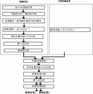
Figure 1 Downlink coding multiplexing scheme
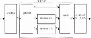
Figure 2 TrCH rate adaptation during puncturing of downlink Turbo coded bits
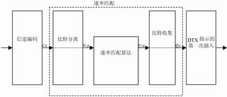
Figure 3 Downstream uncoded and convolutional coding and repeated Turbo coding TrCH rate matching
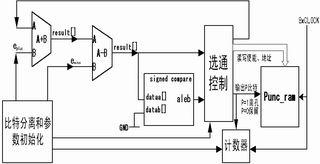
Figure 4 Generating drilling pattern
The rate adaptation algorithm describes that the number of bits in different transmission time intervals on a transmission channel may be different, but the uplink and downlink have certain requirements for the bit rate of transmission: if the number of bits in the downlink is lower than the minimum value Will be interrupted; the number of bits in each transmission time interval in the uplink is different, but it is necessary to ensure that the total bit rate after the second interleaving is equal to the total bit rate of the allocated dedicated physical channel. Therefore, some bits on the transmission channel need to be repeated or chiseled. Rate adaptation means that the data bits on the transmission channel are punctured (Puncturing) or repeated (RepeaTIng), so that the channel mapping reaches the bit rate required by the transmission format. "Punching" is to cut bits at certain positions according to a certain algorithm; "repeat" is to insert repeated bits at certain positions according to a certain algorithm.
The bits before rate matching are recorded as: xi1, xi2, xi3, k, xixi where i is the TrCH number and the rate matching parameters are Xi, eini, eplus, and eminus.
eini: initialization error, the initial value of the error e in the algorithm;
eminus: subtraction error, the subtraction value of error e in the algorithm;
eplus: addition error, the added value of error e in the algorithm;
N: the amount of data, that is, the amount of data before rate adaptation.
The rules for rate matching are as follows:
if to perform "drilling" operation
e = eini Initialize the deviation between the current and required drilling ratio
m = 1 Current bit index number
do while m <= N
e = e-eminus modification error
if e <= 0 then check if m is the bit number that should be cut off
e = e + eplus change error
end if
m = m + 1 to judge the next bit
end do
else
e = eini initializes the current deviation from the required drilling ratio
m = 1 Current bit index number
do while m <= N
e = e-eminus modification error
do while e <= 0 checks whether bit m is a bit number that should be repeated
e = e + eplus change error
end do
m = m + 1 to judge the next bit
end do
end if
This adaptation algorithm is applicable to both uplink and downlink. The 3GPP agreement stipulates the use objects and scope of the "hole drilling" and "repetition" algorithms. The turbo coded system bits are not allowed to be chiseled out. Therefore, if the turbo coded data is "chiseled", the system bit and the parity bit should be distinguished first, and only the parity bit should be chiseled ; However, if the turbo-encoded data is "repetitive" and the convolution-encoded data is "chiseled" or "repetitive", it does not distinguish between systematic bits and check bits. The rate matching in the above cases is shown in Figure 2 and Figure 3.
In addition, the algorithm for determining the parameters given by the protocol varies according to the encoding method and the link. In other words, Turbo coding and convolutional coding, downlink and uplink differ in the algorithm for determining the adaptation parameters. The specific determination algorithm can refer to the corresponding protocol of 3G.
The FPGA implementation of rate adaptation found that through the study of the encoding multiplexing scheme, directly processing the various steps of the data stream (a total of about 11 steps) according to the protocol flow will greatly increase the complexity of the system, so that between each step The data needs to be cached, and the highest rate supported by the system in the mobile environment can reach 384Kbps. For the service with TTI = 20ms, the average buffer required for each step is 7.68K, and the total storage required is huge. And in the middle, the processing delay caused by the frequent writing and reading of data streams is also unbearable. Therefore, if certain steps are combined, unnecessary data access work can be reduced, thereby saving storage and reducing processing delay.
The rate matching on the uplink is performed in units of 10 ms data frames, while the downlink is performed on the data bits of one radio frame in units of TTI. Although the algorithm is consistent, considering the merge of the upstream and downstream steps, the actual processing is still very different. The following line 144Kb / s rate adaptation is used as an example to introduce its FPGA implementation method.
The 144Kb / s rate adaptation process is roughly divided into two modules: a chisel pattern generation module and a reserved bit shift conversion module. In the implementation process, the storage resources used are two RAMs-one to store the "chisel" pattern, the other to store the original data, and two DCFIFO (dual clock FIFO) to store the two frames after the bit collection data.
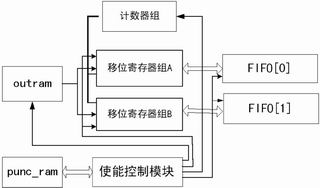
Figure 5 Reserved bit shift conversion
Puncturing pattern generation module Because the 144Kb / s traffic channel coding uses Turbo coding, only the parity bits output by the two component encoders are used during puncturing. Therefore, it is necessary to separate the bits and then perform the puncturing operation in blocks The block is automatically reserved without drilling operations). We use a puncturing pattern control method, all the rate adaptation bits correspond to a P bit, P = 1 means gouging, P = 0 means reservation, in this way, a puncturing pattern is generated to control the movement of reserved bits . The specific implementation block diagram is shown in Figure 4. The main hardware structure includes an adder, a subtractor, a numeric comparator, a counter and a gate control module and parameter initialization module.
The working process of the structure is as follows: First, the bit separation and parameter initialization module mainly completes the module count and the initialization settings of eini, eminus, eplus and other parameters.
At the subtractor side, the current error value e is subtracted from eminus, and this value is sent to both the numerical comparator and the gating control module. The output of the subtractor is compared with the value of 0. If the result is less than zero, the P bit is recorded as 1; if the result is greater than zero, the P bit is recorded as 0. At the same time, the output structure of the subtractor is used as the input value of the current adder. The P bit is written to Punc_ram under the read and write enable generated by the strobe control module and driven by the address signal line. In addition, a counter is used to record the number of bits to control the end time of the entire process. The system clock is 8 times the chip clock, the counter and Punc_ram are controlled synchronously, and the adder, subtractor and comparator do not use synchronous clock delay.
After the reserved bit shift conversion module generates the chisel pattern, the next operation is to move and convert the reserved bits, and perform the first interleaving and radio frame segmentation. According to the 3GPP protocol, for the 144Kb / s service with TTI = 20ms, the interleaving mode is <0,1>, that is, it is output sequentially.
The flow chart of realization is shown in Figure 5. Assuming that the bit stream to be rate-adapted after TURBO encoding is stored in out_ram, the key to the operation here is that the reading of the puncturing pattern and the reading of out_ram should be performed in synchronization (starting at the same clock rising edge), using Punc_ram The output is used as an enable signal for accumulating bits. Use the shift register group and counter to realize bit accumulation, every time when it reaches 16bit, serial-to-parallel conversion is performed, and a fifo write enable pulse is generated, and the content of a word is written into fifo; Data frame), turn to write to the next fifo. By the end of a data frame of 4205bit, the zero-filling of accumulated bits less than 16 indicates that serial-parallel conversion is a word written into fifo.
Resource usage and delay analysis According to the above implementation, the main occupation is storage resources. ESB (Embedded System Block) in modern FPGA can easily implement various types of storage modules, including dual-port RAM, ROM, FIFO And CAM blocks. The following is mainly a delay analysis.
According to the above process, it is possible to roughly estimate the time it takes for a bit from the creation of the "hole" pattern to the completion of the bit transfer. The selected working clock rate is 8 times the chip rate of 3.84MHz, and one clock cycle is about 32.4ns. The adder, subtractor, and gate control in the puncturing pattern module require about 3 clock cycles, and the generation of 9516 puncturing patterns requires approximately 925ns; the reserved bit shifting module is mainly the direct shifting of data bits. In other words, assuming that it is a reserved bit, it takes approximately 9516 + 16 = 9532 clock cycles from the beginning of the move to the final write to the FIFO, which takes about 308 ns. The MAXPUSII simulation is used for the entire process, which takes a total of 1.336ms. Considering the intermediate buffer control and enable control delays, the simulation results are roughly consistent with the calculated values. For the service with TTI = 20ms, it fully meets the processing requirements.
Conclusion
The circuit data service (64K) and packet data service (144K, 384K) of the WCDMA system can carry multimedia services. However, due to the large amount of baseband data processing and the obvious bit shifting operation, one of the core algorithms in encoding multiplexing We used FPGA to implement the rate adaptation algorithm, and merged the previous and next steps appropriately, which greatly shortened the processing time, so that the system reached a high throughput and processing speed, and fully met the requirements of the 3GPP protocol specifications. It proved to be feasible in actual implementation. In addition, the idea of ​​merging modules and generating puncturing patterns for bit accumulation and migration can also be suitable for more complex coding multiplexing schemes in the future.

Follow WeChat

Download Audiophile APP

Follow the audiophile class
related suggestion
For any wireless communication network, the success of the previous network planning directly determines the wireless performance of the network, only through good ...
Abstract: The GPIB interface is a commonly used interface method in test instruments. By setting the interface ...
'+ data.data.username +' '; dom + ='
Best Budget I7 Laptop is everyone eager to. Laptop Intel Core i7 is the No. 1 processor clients choose when they are searching for a performance Gaming Laptop,cause it`s of excellent powering, bigger Solid State Drive, usually 512GB based, full HD 16:9 aspect ratio slimmer display bezels, bigger battery-12000mAh-no need to worry lack of power, fingerprint reader, backlight keyboard, etc. What is intel Core I7 Laptop Price? Usually 300-400usd. You can get Intel i7 11th Generation Laptop, Intel i7 10th Generation Laptop, Intel I5 11th Generation Laptop, Laptop I3 11th Generation,etc. 15.6 or 14 inch all available for i7 processor.
Cooperating with us, you just need to share all your requirements details, like size, cpu, ram, rom, battery, fingerprint, backlight, enter button numbers, SSD+HDD or only SSD ok, if need oem service, if need logo position, special apps preinstall if need, etc. Can provide matched and value feedback in 1-2 working days.
The reason why clients choose us is that just half of DOA than others, longer warranty time, smaller MOQ, fast delivery, competitive cost, good after-sale service, etc.
Laptop Intel Core I7,Intel Core I7 Laptop Price,Best Budget I7 Laptop,Intel I7 11th Generation Laptop,Intel I7 10th Generation Laptop
Henan Shuyi Electronics Co., Ltd. , https://www.sycustomelectronics.com