Definition: not all nanomaterials with dimensions less than 100nm are called nanotechnology
The broad definition of nanotechnology refers to materials with sizes less than 100 nm (nanometers), while the science of researching nanomaterials is commonly referred to as "nanotechnology." Nanotechnology has a wide range of research, including nanophysics, nanochemistry, nanomaterials, nanobiology, nanoelectronics, nanomachining, nanomechanics and nanometerometry. Many cutting-edge research is constantly underway. Let us first understand what is nanotechnology!
The strict definition of nanotechnology must meet the following three conditions simultaneously:
1. The size of the nanomaterial is less than 100 nm.
2. Nanomaterials are small in size and have new properties such as light, electricity, magnetism, sound, chemistry and mechanics.
3. Nanomaterials must have new research value and application.
In other words, only meeting the small size is not the most important condition of nanotechnology, and must have new properties and applications, which is the focus of nanotechnology discussion.
It is worth mentioning that the strict definition of nanotechnology must meet the above three conditions at the same time, but at present, the entire academic community and the industry are using a looser definition, that is, as long as the first condition above is less than 100 nm. This has caused the chaos of everything in the world today. Many manufacturers are ignoring the chaotic situation and abusing the word "nano". This article will help you to use science in a simple sentence to make you a rational nanotechnology judge.
Classification: roughly divided into two important areas of nanomaterials and nanotechnology
The nanotechnology industry is still not complete, and many applications are still in the stage of theoretical research, so it is not easy to classify them completely, but it can be roughly divided into two important areas:
Nano-materials: “final productsâ€, which means that nano-processing technology is used to process materials into products with a size below 100 nm. This product can be called “nano-materialâ€.
Nano-technology: refers to the "processing process", which means the process technology used to process materials into sizes below 100 nm. We call them "nanotechnology."
The relationship between "nanomaterials" and "nanotechnology" is somewhat similar to the relationship between "LEDs" and "devices that produce LEDs". LED factories (eg Sanan Optoelectronics and Mulinsen) are targeting LED equipment vendors (eg : EVECO, North Huachuang or ASM) purchase LED chips or packaging equipment to produce LED devices. Therefore, equipment manufacturers focus on how to design cost-effective processing equipment, while LED manufacturers focus on how to use equipment to produce LEDs. Both play an important role in the LED industry.
By the same token, the focus of nanotechnology discussions is on how to design nanofabrication equipment. The focus of nanomaterials discussion is on how to use nanofabrication equipment to produce nanomaterials, both of which play an important role in the nanotechnology industry.
Type: Nanomaterials are divided into two-dimensional, one-dimensional, zero-dimensional by appearance geometry
The traditional general size material is called "Bulk". Its structure is that the X-axis, Y-axis and Z-axis in three-dimensional space can extend infinitely, as shown in Figure 1 (a), while nano-materials can Simply divided into three dimensions, one-dimensional, zero-dimensional, etc. by the geometry of the appearance:
Two-dimensional: The X-axis and the Y-axis can extend infinitely, but the Z-axis is very small (less than 100 nm). As shown in Figure 1 (b), the two-dimensional nanostructure is called "Nano thin film". ) or "Quantum well".
One-dimensional: The X-axis can extend infinitely, but the Y-axis and the Z-axis are very small (less than 100 nm). As shown in Figure 1 (c), the one-dimensional nanostructure is longer. (Nanowires), the shorter one is called "Nanorods", and the hollow one is called "Nanotube".
Zero-dimensional: The X-axis, Y-axis, and Z-axis are very small (less than 100 nm). As shown in Figure 1 (d), the zero-dimensional nanostructures are called "Nanoparticles" or "Quantum." Quantum dots.
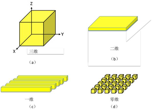
Figure 1 The geometry of nanomaterials
Photoelectric characteristics: LED, LD luminescent layer and quantum dot technology
First, the core principle of LED/LD luminescent layer and quantum dot display technology: quantum confinement effect
The physical properties of materials are mostly determined by electrons and holes. For example, "Debye Debye Length" is used to describe the length of the force between electrons and electrons in a material. "de Broglie De Broglie Wavelength" is used to define materials. The particle properties and wave properties, because the bulk size of the traditional three-dimensional space is much larger than the physical feature length of these electrons and holes, the physical properties can be explained by classical physics, but when the size of the material is small When the wavelength is below 100 nm, it will be close to the Debye length and the De Broglie wavelength, so a "quantum confinement effect" will occur.
Regarding the quantum limitation effect, I believe that many friends who have studied university physics should not be unfamiliar. I don't like to write a large number of formulas, especially the difficult and difficult to understand Schrödinger equation. I have compiled a PPT textbook on quantum physics. I found that using this textbook to make students understand quantum physics is very difficult, not to mention using text to help students who have not studied university physics to teach this difficult quantum bone. Now I try to explain this effect with pictures and words. :
In the microscopic world, especially at the nanoscale, all light and electricity phenomena are different from the large-scale world we see, as shown in Figure 2(a) (the formula can't be understood and can jump over) According to the solution of the Schrödinger equation wave function, under the quantum scale (L), the energy state ΔE of electrons and holes will be different, perhaps it will be at the energy level Eo, maybe at 4Eo. The location, maybe at 9Eo or 16Eo.... . Because of the difference in physical size, the energy level of the electrons in the material will change accordingly, and the material properties presented will be greatly different from the original material properties, as shown in Figure 2(b). The frequency is no longer the energy band gap property Eg of the material itself, but the band gap is wider (Eg+ΔEc+ΔEv), and the energy becomes stronger, so the wavelength of the light is shortened, because electrons and holes are confined to the nanomaterial. The formation of a self-organized steady state, resulting in changes in the photoelectric properties, such effects are called quantum confinement effects.
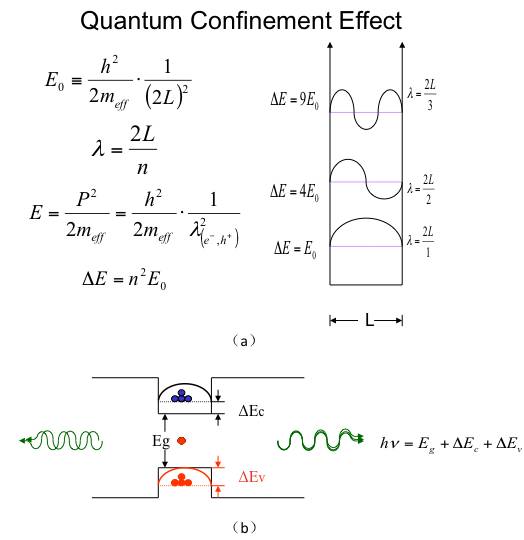
Figure 2 Quantum Limitation Effects at the Nanoscale
The most obvious feature of the quantum confinement effect is that the smaller the size of the nanomaterial, the stronger the luminescence energy of the material, and the stronger the energy, the shorter the wavelength of the luminescence (blue). This phenomenon is called "blue shift".
As shown in Figure 3, the wavelengths of light of different colors are different, the wavelength of light is the color, the wavelength of red light is the longest in visible light, the second is green light, and the blue light is the shortest. In other words, when the size of nano material is large, it is luminous. The energy is lower, the color is red light (the longest wavelength); when the size of the nano material becomes smaller, the luminescence energy becomes stronger, the color is green light (the wavelength is second); when the size of the nano material is smaller, the luminescence energy is stronger, The color is blue (the shortest wavelength).
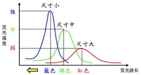
Figure 3 quantum confinement effect
Second, LED and LD epitaxy the most critical luminescent layer: nano-film and quantum well
1, type and characteristics
The two-dimensional nanostructure is called "Nano thin film" and refers to a film with a thickness of 100 nm or less. As shown in the LED structure of Figure 4 (a), the semiconductor material has special photoelectric characteristics, so it is common. Most of the nano-films are made of semiconductor materials, such as silicon, gallium arsenide, gallium nitride or indium phosphide. They have excellent photoelectric properties and can be used in the photovoltaic technology industry.
When we stack many layers of semiconductor nanofilms with different materials, we can form "quantum wells". For example, gallium arsenide, indium gallium arsenide, and arsenic are grown on gallium arsenide wafers. Nano-films of aluminum gallium or nano-films of gallium nitride, indium gallium nitride and aluminum gallium nitride grown on sapphire are all quantum well structures, as shown in the quantum well LED light-emitting layer structure shown in Figure 4(b). Studies have shown that LED light-emitting diodes or LD laser diode components with quantum well structures have better luminous efficiency.
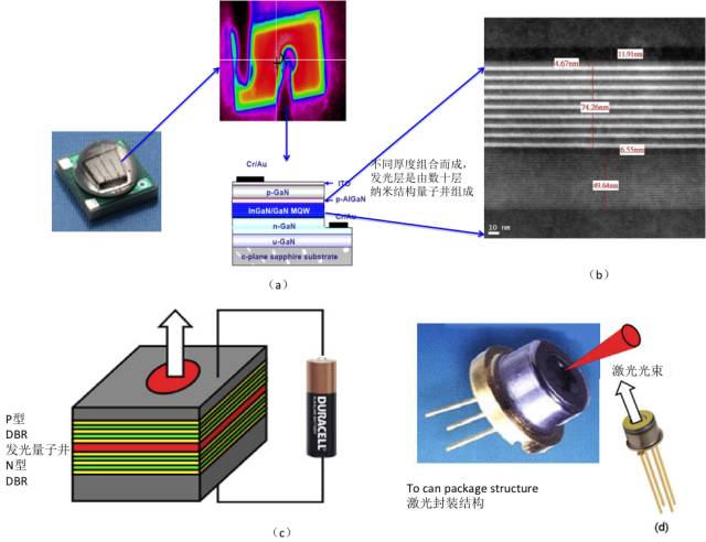
Figure 4 Definition and application of nano-film and quantum well
2. Quantum well application examples
Figure 4(c) shows the "Quantum Well Laser Diode" made by using a multi-layer quantum well structure. The scientists call it "VCSEL: Vertical Cavity Surface Emitting Laser". It is a product that has been mass-produced at present, and its appearance is shown in Figure 4(d). This structure is commonly used in light sources for optical communication.
The laser in the picture is made of gallium arsenide wafer. The upper and lower sides are metal electrodes. The upper side is connected to the positive electrode of the battery, and the lower side is connected to the negative electrode of the battery. The upper and lower sides are dozens of N-type and P-type nano-films, and the darker parts. Representing a larger index of refraction (Index), the part with a lighter color represents a smaller index of refraction (Index). This component, which is composed of many layers of films with different refractive indices, is a very important optical structure, which we call "Brag reflection layer DBR grating (Grating)"; the center is a nano-film, because it is sandwiched between the upper and lower gratings, so the structure of the quantum well, called the "quantum well luminescence area", is the main illuminating area of ​​the laser The type of semiconductor material in this layer determines the color and intensity of the laser light. Since the vertical cavity surface-emitting laser (VCSEL) uses a quantum well structure, it can increase luminous efficiency and have excellent photoelectric characteristics.
3. Nano film preparation method
Nanocrystalline films can be fabricated using single crystal or polycrystalline thin film growth techniques, but nanofilms obtained by methods such as heating evaporation, electron beam evaporation, sputtering, and plasma chemical vapor deposition (PECVD) are of poor quality. At present, most of the use of relatively strict process conditions, relatively high cost of molecular beam epitaxy (MBE) or organic chemical vapor deposition (MOCVD) to make nano-film, molecular beam epitaxy (MBE) can be atomic under ultra-high vacuum The layer layer grows on the surface of the wafer, so it can be controlled very accurately. It can make a single layer of nano-film, or it can make a multi-layer quantum well structure.
A new ace of display technology: nanoparticles and quantum dots
1. Quantum dot effect of LED and LD on the luminescent layer
The zero-dimensional nanostructure is called "nanoparticle" and refers to particles with a particle size (diameter) of less than 100 nm. As shown in Figure 5 (a), the semiconductor material has special photoelectric properties, so the common nanometer. Most of the particles are made of semiconductor materials, such as silicon, gallium arsenide, gallium nitride, etc., which have superior photoelectric properties and are used in the photovoltaic technology industry.
When we use nano-films of semiconductors to cover the nanoparticles, we will form a "quantum dot" structure. For example, after the gallium nitride substrate is grown on the sapphire substrate, the indium gallium nitride light-emitting layer is caused by temperature variation. The phase separation effect, the indium-rich indium gallium nitride nanoparticles appear on the luminescent layer, and then a layer of "aluminum gallium nitride or gallium nitride" nano-film is covered. Quantum well structure of indium-rich quantum dots.
As shown in Figure 5(b), the Nobel Prize winner in physics, also the inventor of Indium Gallium Nitride Blue LED, Professor Nakamura Shuji believes that indium gallium nitride LEDs or laser LD optoelectronic devices with quantum dot structure have better luminous efficiency. .
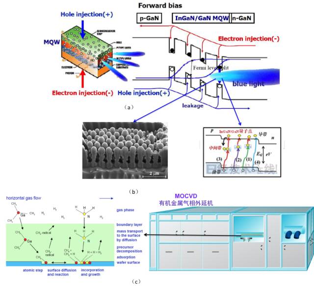
Figure 5. Using MOCVD to make nanoparticles and quantum dots
2. Preparation method of nanoparticles
Nanoparticles can be fabricated using thin film growth techniques, but they must be combined with appropriate devices to control different temperatures and pressures to aid in the formation of nanoparticles. Otherwise, only nanofilms can be formed, such as: thermal evaporation, electron beam evaporation, splashing. Sputter, plasma chemical vapor deposition (PECVD), molecular beam epitaxy (MBE), organic chemical vapor deposition (MOCVD), and the like. For example, as shown in Figure 5(c), if indium gallium nitride nanoparticles are to be prepared, organic chemical vapor deposition (MOCVD) can be used to mix ammonia with organometallic trimethylgallium and trimethylindium, respectively. Nitrogen gas is introduced into the reaction chamber to control different pressures and temperatures to obtain indium gallium nitride nanoparticles, which can emit very bright blue or green light.
3, quantum dot display technology: the opportunity to become the OLED after the pursuit of the dream display technology
Due to the quantum confinement effect, nanoparticles of different sizes emit fluorescence of different wavelengths (color). For example, cadmium selenide (CdSe) emits red fluorescence when it is 10 nm in diameter, emits green fluorescence when it is 5 nm in diameter, and emits blue fluorescence when it is 2 nm in diameter. As shown in Figure 6(a), and its luminous intensity is more than 10 times higher than that of traditional organic fluorescent materials, and compared with the current display technology, quantum dots have self-luminous, high contrast, wide viewing angle and light and flexible. And so on, will have the opportunity to become the dream display technology in the market after the OLED.
Recently, the display technology on the market is a bit of a fascinating dance. 4k8K LCD, OLED, Micro LED, laser TV and quantum dot QLED contend. The quantum dot display technology is still not very mature, but why there are still many quantum dot markers on the market. QLED TV?
As shown in Figure 6(b), the current quantum dot TV uses the characteristics of the quantum dot luminescence spectrum to emit high-purity colors, thereby achieving better full-color display, adding quantum dots to the LCD backlight, and quantum. The point absorbing light from the backlight, re-emitting high-purity light with photoluminescence (PL), becoming a solid color backlight, and producing high-color display technology. Recently, TCL and QD Vision jointly launched 55å‹4k quantum dot TV. Using this technology, however, such quantum dot photoluminescence technology is only a traditional LCD technology plus quantum dot film as a color adjustment, although it brings excellent color characteristics, but is essentially limited by LCD display technology. Still can not enjoy the advantages of high contrast, wide viewing angle and thin and flexible!
Because everyone is unfamiliar with this technology, and has no ability to understand such a deep physics, TV manufacturers will attract the attention of ordinary people with the nouns of high-tech quantum dots. In fact, the current QLED TV is still a modified version of LCD TV!
The most common quantum dot structure is shown in Figure 6(c). It generally contains an inorganic semiconductor core layer (core, about 1 to 10 nm in diameter), a wide band gap inorganic semiconductor shell (Shell), and the outermost organic ligand ( Ligand), the core layer is the main luminescent layer of quantum dots. Different kinds of materials such as CdSe, CdS, InP and ZnSe are used to synthesize different sizes. The color of the quantum dots can be adjusted, and the time, temperature and concentration of the reactants can be used. In addition, after the synthesis of the filter screen, the size of the quantum dots can be made more uniform and uniform, and a purer light color can be emitted. The shell layer covers the core layer, isolates oxygen and moisture, repairs the core layer defects, and improves the luminous efficiency. The outermost organic ligand can disperse the quantum dots in different non-polar organic solvents, which is beneficial to the use of solution processes. To make quantum dot light-emitting devices.
In the future, QLED devices, process methods and light-emitting structures will be closer to current OLEDs. As shown in Figure 6(d), electroluminescence is used. The biggest difference is that QLEDs use quantum dots as luminescent materials, electrons and vacancies. The hole transport layer can use an organic material close to the OLED to make a new generation of flexible display. Of course, the current structural efficiency is still very low, so in order to improve the QLED efficiency, the organic material plus the zinc oxide ZnO electron transport layer and the nickel oxide NiO The hole transport layer is a better choice for improving efficiency. The latest achievement is that the team of Professor Peng Xiaogang from Zhejiang University uses the organic material PMMA as the buffer structure layer of the zinc oxide ZnO electron conduction layer and the quantum dot light-emitting layer, which can achieve the efficiency close to OLED. It is one of the world's most advanced QLED technology leaders.
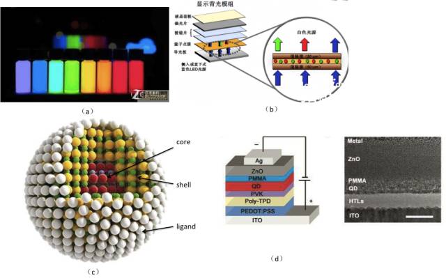
Figure 6. Application of Nanoparticles and Quantum Dots
The only drawback of nanotechnology!
The magic of semiconductor integrated circuit technology: quantum wear-through effect
"Insulator" is a solid that is not easily conductive, such as plastic or ceramic, so electrons cannot penetrate the insulator, but when the size of the material is less than 100 nm, because it is too thin, scientists have found that electrons can penetrate the insulator arbitrarily. We call it the "quantum tunneling effect". In other words, plastics, ceramics, which are originally insulators in bulk materials, are no longer when their size is less than 100 nm. Insulators are gone.
In the traditional integrated circuit process, CMOS must use "silicon oxide" to make the gate, because silicon oxide is a good insulator, but when the gate width of CMOS is less than 100nm, the thickness of silicon oxide may be only 10nm, due to Quantum tunneling, such thin silicon oxide can cause electrons to penetrate arbitrarily and cannot be insulated. Therefore, fabs must use other materials instead of silicon oxide. For fabs, it is necessary to add new processes to solve the problem. At this time, nano is a trouble that must be solved. From this example, it can be found that not all things are made into nanometers. It is necessary to look at what products are applied. "The big one is big, the small one is small" is the best policy.
This article is about the superior performance of optoelectronic components at the nanometer scale. In fact, nanomaterials have many magical effects. For example, the surface and interface effects of nanotechnology can make nano ceramic powder coatings. (Paint), using this nano-ceramic powder coated on the fuselage of the fighter aircraft, can absorb the electromagnetic waves of all radars, the US F35 and China æ¼20 stealth fighters are using this technology to get, due to limited space, only next time Science and technology in this area is for everyone!
It is such a magic at the nanometer scale that it is worth exploring!
Do you understand about nano?
Definition: not all nanomaterials with dimensions less than 100nm are called nanotechnology
The broad definition of nanotechnology refers to materials with sizes less than 100 nm (nanometers), while the science of researching nanomaterials is commonly referred to as "nanotechnology." Nanotechnology has a wide range of research, including nanophysics, nanochemistry, nanomaterials, nanobiology, nanoelectronics, nanomachining, nanomechanics and nanometerometry. Many cutting-edge research is constantly underway. Let us first understand what is nanotechnology!
The strict definition of nanotechnology must meet the following three conditions simultaneously:
1. The size of the nanomaterial is less than 100 nm.
2. Nanomaterials are small in size and have new properties such as light, electricity, magnetism, sound, chemistry and mechanics.
3. Nanomaterials must have new research value and application.
In other words, only meeting the small size is not the most important condition of nanotechnology, and must have new properties and applications, which is the focus of nanotechnology discussion.
It is worth mentioning that the strict definition of nanotechnology must meet the above three conditions at the same time, but at present, the entire academic community and the industry are using a looser definition, that is, as long as the first condition above is less than 100 nm. This has caused the chaos of everything in the world today. Many manufacturers are ignoring the chaotic situation and abusing the word "nano". This article will help you to use science in a simple sentence to make you a rational nanotechnology judge.
Classification: roughly divided into two important areas of nanomaterials and nanotechnology
The nanotechnology industry is still not complete, and many applications are still in the stage of theoretical research, so it is not easy to classify them completely, but it can be roughly divided into two important areas:
Nano-materials: “final productsâ€, which means that nano-processing technology is used to process materials into products with a size below 100 nm. This product can be called “nano-materialâ€.
Nano-technology: refers to the "processing process", which means the process technology used to process materials into sizes below 100 nm. We call them "nanotechnology."
The relationship between "nanomaterials" and "nanotechnology" is somewhat similar to the relationship between "LEDs" and "devices that produce LEDs". LED factories (eg Sanan Optoelectronics and Mulinsen) are targeting LED equipment vendors (eg : EVECO, North Huachuang or ASM) purchase LED chips or packaging equipment to produce LED devices. Therefore, equipment manufacturers focus on how to design cost-effective processing equipment, while LED manufacturers focus on how to use equipment to produce LEDs. Both play an important role in the LED industry.
By the same token, the focus of nanotechnology discussions is on how to design nanofabrication equipment. The focus of nanomaterials discussion is on how to use nanofabrication equipment to produce nanomaterials, both of which play an important role in the nanotechnology industry.
Type: Nanomaterials are divided into two-dimensional, one-dimensional, zero-dimensional by appearance geometry
The traditional general size material is called "Bulk". Its structure is that the X-axis, Y-axis and Z-axis in three-dimensional space can extend infinitely, as shown in Figure 1 (a), while nano-materials can Simply divided into three dimensions, one-dimensional, zero-dimensional, etc. by the geometry of the appearance:
Two-dimensional: The X-axis and the Y-axis can extend infinitely, but the Z-axis is very small (less than 100 nm). As shown in Figure 1 (b), the two-dimensional nanostructure is called "Nano thin film". ) or "Quantum well".
One-dimensional: The X-axis can extend infinitely, but the Y-axis and the Z-axis are very small (less than 100 nm). As shown in Figure 1 (c), the one-dimensional nanostructure is longer. (Nanowires), the shorter one is called "Nanorods", and the hollow one is called "Nanotube".
Zero-dimensional: The X-axis, Y-axis, and Z-axis are very small (less than 100 nm). As shown in Figure 1 (d), the zero-dimensional nanostructures are called "Nanoparticles" or "Quantum." Quantum dots.
Figure 1 The geometry of nanomaterials
Photoelectric characteristics: LED, LD luminescent layer and quantum dot technology
First, the core principle of LED/LD luminescent layer and quantum dot display technology: quantum confinement effect
The physical properties of materials are mostly determined by electrons and holes. For example, "Debye Debye Length" is used to describe the length of the force between electrons and electrons in a material. "de Broglie De Broglie Wavelength" is used to define materials. The particle properties and wave properties, because the bulk size of the traditional three-dimensional space is much larger than the physical feature length of these electrons and holes, the physical properties can be explained by classical physics, but when the size of the material is small When the wavelength is below 100 nm, it will be close to the Debye length and the De Broglie wavelength, so a "quantum confinement effect" will occur.
Regarding the quantum limitation effect, I believe that many friends who have studied university physics should not be unfamiliar. I don't like to write a large number of formulas, especially the difficult and difficult to understand Schrödinger equation. I have compiled a PPT textbook on quantum physics. I found that using this textbook to make students understand quantum physics is very difficult, not to mention using text to help students who have not studied university physics to teach this difficult quantum bone. Now I try to explain this effect with pictures and words. :
In the microscopic world, especially at the nanoscale, all light and electricity phenomena are different from the large-scale world we see, as shown in Figure 2(a) (the formula can't be understood and can jump over) According to the solution of the Schrödinger equation wave function, under the quantum scale (L), the energy state ΔE of electrons and holes will be different, perhaps it will be at the energy level Eo, maybe at 4Eo. The location, maybe at 9Eo or 16Eo.... . Because of the difference in physical size, the energy level of the electrons in the material will change accordingly, and the material properties presented will be greatly different from the original material properties, as shown in Figure 2(b). The frequency is no longer the energy band gap property Eg of the material itself, but the band gap is wider (Eg+ΔEc+ΔEv), and the energy becomes stronger, so the wavelength of the light is shortened, because electrons and holes are confined to the nanomaterial. The formation of a self-organized steady state, resulting in changes in the photoelectric properties, such effects are called quantum confinement effects.
Figure 2 Quantum Limitation Effects at the Nanoscale
The most obvious feature of the quantum confinement effect is that the smaller the size of the nanomaterial, the stronger the luminescence energy of the material, and the stronger the energy, the shorter the wavelength of the luminescence (blue). This phenomenon is called "blue shift".
As shown in Figure 3, the wavelengths of light of different colors are different, the wavelength of light is the color, the wavelength of red light is the longest in visible light, the second is green light, and the blue light is the shortest. In other words, when the size of nano material is large, it is luminous. The energy is lower, the color is red light (the longest wavelength); when the size of the nano material becomes smaller, the luminescence energy becomes stronger, the color is green light (the wavelength is second); when the size of the nano material is smaller, the luminescence energy is stronger, The color is blue (the shortest wavelength).
Figure 3 quantum confinement effect
Second, LED and LD epitaxy the most critical luminescent layer: nano-film and quantum well
1, type and characteristics
The two-dimensional nanostructure is called "Nano thin film" and refers to a film with a thickness of 100 nm or less. As shown in the LED structure of Figure 4 (a), the semiconductor material has special photoelectric characteristics, so it is common. Most of the nano-films are made of semiconductor materials, such as silicon, gallium arsenide, gallium nitride or indium phosphide. They have excellent photoelectric properties and can be used in the photovoltaic technology industry.
When we stack many layers of semiconductor nanofilms with different materials, we can form "quantum wells". For example, gallium arsenide, indium gallium arsenide, and arsenic are grown on gallium arsenide wafers. Nano-films of aluminum gallium or nano-films of gallium nitride, indium gallium nitride and aluminum gallium nitride grown on sapphire are all quantum well structures, as shown in the quantum well LED light-emitting layer structure shown in Figure 4(b). Studies have shown that LED light-emitting diodes or LD laser diode components with quantum well structures have better luminous efficiency.
Figure 4 Definition and application of nano-film and quantum well
2. Quantum well application examples
Figure 4(c) shows the "Quantum Well Laser Diode" made by using a multi-layer quantum well structure. The scientists call it "VCSEL: Vertical Cavity Surface Emitting Laser". It is a product that has been mass-produced at present, and its appearance is shown in Figure 4(d). This structure is commonly used in light sources for optical communication.
The laser in the picture is made of gallium arsenide wafer. The upper and lower sides are metal electrodes. The upper side is connected to the positive electrode of the battery, and the lower side is connected to the negative electrode of the battery. The upper and lower sides are dozens of N-type and P-type nano-films, and the darker parts. Representing a larger index of refraction (Index), the part with a lighter color represents a smaller index of refraction (Index). This component, which is composed of many layers of films with different refractive indices, is a very important optical structure, which we call "Brag reflection layer DBR grating (Grating)"; the center is a nano-film, because it is sandwiched between the upper and lower gratings, so the structure of the quantum well, called the "quantum well luminescence area", is the main illuminating area of ​​the laser The type of semiconductor material in this layer determines the color and intensity of the laser light. Since the vertical cavity surface-emitting laser (VCSEL) uses a quantum well structure, it can increase luminous efficiency and have excellent photoelectric characteristics.
3. Nano film preparation method
Nanocrystalline films can be fabricated using single crystal or polycrystalline thin film growth techniques, but nanofilms obtained by methods such as heating evaporation, electron beam evaporation, sputtering, and plasma chemical vapor deposition (PECVD) are of poor quality. At present, most of the use of relatively strict process conditions, relatively high cost of molecular beam epitaxy (MBE) or organic chemical vapor deposition (MOCVD) to make nano-film, molecular beam epitaxy (MBE) can be atomic under ultra-high vacuum The layer layer grows on the surface of the wafer, so it can be controlled very accurately. It can make a single layer of nano-film, or it can make a multi-layer quantum well structure.
A new ace of display technology: nanoparticles and quantum dots
1. Quantum dot effect of LED and LD on the luminescent layer
The zero-dimensional nanostructure is called "nanoparticle" and refers to particles with a particle size (diameter) of less than 100 nm. As shown in Figure 5 (a), the semiconductor material has special photoelectric properties, so the common nanometer. Most of the particles are made of semiconductor materials, such as silicon, gallium arsenide, gallium nitride, etc., which have superior photoelectric properties and are used in the photovoltaic technology industry.
When we use nano-films of semiconductors to cover the nanoparticles, we will form a "quantum dot" structure. For example, after the gallium nitride substrate is grown on the sapphire substrate, the indium gallium nitride light-emitting layer is caused by temperature variation. The phase separation effect, the indium-rich indium gallium nitride nanoparticles appear on the luminescent layer, and then a layer of "aluminum gallium nitride or gallium nitride" nano-film is covered. Quantum well structure of indium-rich quantum dots.
As shown in Figure 5(b), the Nobel Prize winner in physics, also the inventor of Indium Gallium Nitride Blue LED, Professor Nakamura Shuji believes that indium gallium nitride LEDs or laser LD optoelectronic devices with quantum dot structure have better luminous efficiency. .
Figure 5. Using MOCVD to make nanoparticles and quantum dots
2. Preparation method of nanoparticles
Nanoparticles can be fabricated using thin film growth techniques, but they must be combined with appropriate devices to control different temperatures and pressures to aid in the formation of nanoparticles. Otherwise, only nanofilms can be formed, such as: thermal evaporation, electron beam evaporation, splashing. Sputter, plasma chemical vapor deposition (PECVD), molecular beam epitaxy (MBE), organic chemical vapor deposition (MOCVD), and the like. For example, as shown in Figure 5(c), if indium gallium nitride nanoparticles are to be prepared, organic chemical vapor deposition (MOCVD) can be used to mix ammonia with organometallic trimethylgallium and trimethylindium, respectively. Nitrogen gas is introduced into the reaction chamber to control different pressures and temperatures to obtain indium gallium nitride nanoparticles, which can emit very bright blue or green light.
3, quantum dot display technology: the opportunity to become the OLED after the pursuit of the dream display technology
Due to the quantum confinement effect, nanoparticles of different sizes emit fluorescence of different wavelengths (color). For example, cadmium selenide (CdSe) emits red fluorescence when it is 10 nm in diameter, emits green fluorescence when it is 5 nm in diameter, and emits blue fluorescence when it is 2 nm in diameter. As shown in Figure 6(a), and its luminous intensity is more than 10 times higher than that of traditional organic fluorescent materials, and compared with the current display technology, quantum dots have self-luminous, high contrast, wide viewing angle and light and flexible. And so on, will have the opportunity to become the dream display technology in the market after the OLED.
Recently, the display technology on the market is a bit of a fascinating dance. 4k8K LCD, OLED, Micro LED, laser TV and quantum dot QLED contend. The quantum dot display technology is still not very mature, but why there are still many quantum dot markers on the market. QLED TV?
As shown in Figure 6(b), the current quantum dot TV uses the characteristics of the quantum dot luminescence spectrum to emit high-purity colors, thereby achieving better full-color display, adding quantum dots to the LCD backlight, and quantum. The point absorbing light from the backlight, re-emitting high-purity light with photoluminescence (PL), becoming a solid color backlight, and producing high-color display technology. Recently, TCL and QD Vision jointly launched 55å‹4k quantum dot TV. Using this technology, however, such quantum dot photoluminescence technology is only a traditional LCD technology plus quantum dot film as a color adjustment, although it brings excellent color characteristics, but is essentially limited by LCD display technology. Still can not enjoy the advantages of high contrast, wide viewing angle and thin and flexible!
Because everyone is unfamiliar with this technology, and has no ability to understand such a deep physics, TV manufacturers will attract the attention of ordinary people with the nouns of high-tech quantum dots. In fact, the current QLED TV is still a modified version of LCD TV!
The most common quantum dot structure is shown in Figure 6(c). It generally contains an inorganic semiconductor core layer (core, about 1 to 10 nm in diameter), a wide band gap inorganic semiconductor shell (Shell), and the outermost organic ligand ( Ligand), the core layer is the main luminescent layer of quantum dots. Different kinds of materials such as CdSe, CdS, InP and ZnSe are used to synthesize different sizes. The color of the quantum dots can be adjusted, and the time, temperature and concentration of the reactants can be used. In addition, after the synthesis of the filter screen, the size of the quantum dots can be made more uniform and uniform, and a purer light color can be emitted. The shell layer covers the core layer, isolates oxygen and moisture, repairs the core layer defects, and improves the luminous efficiency. The outermost organic ligand can disperse the quantum dots in different non-polar organic solvents, which is beneficial to the use of solution processes. To make quantum dot light-emitting devices.
In the future, QLED devices, process methods and light-emitting structures will be closer to current OLEDs. As shown in Figure 6(d), electroluminescence is used. The biggest difference is that QLEDs use quantum dots as luminescent materials, electrons and vacancies.ç©´ä¼ è¾“å±‚å¯ä»¥ä½¿ç”¨è·ŸOLED接近的有机æ料,åšå‡ºæ–°ä¸€ä»£æŸ”性显示器,当然目å‰è¿™æ ·çš„结构效率还是很低,所以为了æå‡QLED效率,有机ææ–™åŠ ä¸Šæ°§åŒ–é”ŒZnO的电åä¼ è¾“å±‚ä¸Žæ°§åŒ–é•NiOç©ºç©´ä¼ è¾“å±‚æ˜¯æå‡æ•ˆçŽ‡çš„比较好的选择,目å‰æœ€æ–°çš„æˆæžœæ˜¯æµ™æ±Ÿå¤§å¦å½ç¬‘刚教授团队利用有机ææ–™PMMA作为氧化锌ZnO电åä¼ å¯¼å±‚ä¸Žé‡å点å‘光层的缓冲结构层,å¯ä»¥è¾¾åˆ°æŽ¥è¿‘OLED的效率,是目å‰ä¸–界最å‰æ²¿çš„QLED技术领航者之一。
图å…纳米粒å与é‡å点的应用
纳米技术唯一的缺点ï¼
åŠå¯¼ä½“集æˆç”µè·¯æŠ€æœ¯çš„é”咒:é‡åç©¿éšæ•ˆåº”
「ç»ç¼˜ä½“ã€æ˜¯ä¸å®¹æ˜“导电的固体,例如:塑料ã€é™¶ç“·ï¼Œå› æ¤ç”µåæ— æ³•ç©¿é€ç»ç¼˜ä½“,但是当æ料的尺寸å°äºŽ100nmä»¥ä¸‹æ—¶ï¼Œå› ä¸ºå®žåœ¨æ˜¯å¤ªè–„äº†ï¼Œç§‘å¦å®¶å‘现电å竟然å¯ä»¥ä»»æ„地穿é€ç»ç¼˜ä½“,我们称为「é‡å穿隧效应(Quantum tunneling effect)ã€ï¼Œæ¢å¥è¯è¯´ï¼Œå¡‘æ–™ã€é™¶ç“·è¿™ç§åŽŸæœ¬åœ¨å—æ(Bulk)时是ç»ç¼˜ä½“çš„æ料,当它的尺寸å°äºŽ100nm以下时就ä¸å†æ˜¯ç»ç¼˜ä½“了。
ç”±äºŽåœ¨ä¼ ç»Ÿé›†æˆç”µè·¯åˆ¶ç¨‹ä¸ï¼ŒCMOS必须使用「氧化硅ã€æ¥åˆ¶ä½œé—¸æžï¼Œå› 为氧化硅是很好的ç»ç¼˜ä½“,但是当CMOSçš„é—¸æžçº¿å®½å°äºŽ100nm时,氧化硅的厚度å¯èƒ½åªæœ‰10nm,由于é‡å穿隧效应,这么薄的氧化硅会使电åä»»æ„地穿é€è€Œæ— 法ç»ç¼˜ï¼Œå› æ¤æ™¶åœ†åŽ‚必须使用其他ææ–™æ¥å–代氧化硅,对晶圆厂æ¥è¯´æ˜¯å¿…é¡»å¢žåŠ æ–°åˆ¶ç¨‹æ¥è§£å†³é—®é¢˜çš„æˆæœ¬ï¼Œè¿™ä¸ªæ—¶å€™çº³ç±³å而是个必须解决的麻烦。由这个例åå¯ä»¥å‘现,并ä¸æ˜¯æ‰€æœ‰çš„东西åšæˆçº³ç±³å°±å¥½ï¼Œå¿…é¡»è¦çœ‹åº”用在什么产å“,「该大就大,该å°åˆ™å°ã€æ‰æ˜¯ä¸Šç–。
è¿™ç¯‡æ–‡ç« æ˜¯å…³äºŽåœ¨çº³ç±³å°ºåº¦ä¸‹ï¼Œå…‰ç”µå…ƒå™¨ä»¶å‘ˆçŽ°å‡ºä¼˜è¶Šçš„æ€§èƒ½ï¼Œå…¶å®žçº³ç±³æ料还有很多神奇的效果,例如纳米技术之表é¢ä¸Žç•Œé¢æ•ˆåº”(Surface and interface effect)å¯ä»¥åˆ¶ä½œçº³ç±³é™¶ç“·ç²‰æœ«çš„涂料(油漆),利用这ç§çº³ç±³é™¶ç“·ç²‰æœ«æ¶‚布在战机的机身,å¯ä»¥å¸æ”¶æ‰€æœ‰é›·è¾¾çš„电ç£æ³¢ï¼Œç¾Žå›½F35与ä¸å›½æ¼20éšå½¢æˆ˜æ–—机就是利用这ç§æŠ€æœ¯æžå®šçš„,由于篇幅有é™ï¼Œåªèƒ½ä¸‹æ¬¡å†ç§‘普这方é¢çš„技术给大家了ï¼
åœ¨çº³ç±³å°ºåº¦ä¸‹å°±æ˜¯è¿™æ ·ç¥žå¥‡ï¼Œå€¼å¾—æˆ‘ä»¬åŽ»æŽ¢ç´¢ï¼
å…³äºŽçº³ç±³ï¼Œä½ æ‡‚äº†å—?
Gas Explosion-Proof Motor,Explosion Proof Motors,Gas Explosion Proof Motors,Explosion Proof Electric Motor
Yizheng Beide Material Co., Ltd. , https://www.beidevendor.com