At present, with the intensification of the energy crisis, white LED-based lighting technology has received more and more attention, and its application range has become more and more extensive, and it is gradually replacing traditional light sources [1]. LED lighting differs from conventional light sources in that the LED chips cannot dissipate the heat generated during operation by means of thermal radiation. On the other hand, LED chip life, luminous flux, color coordinates and other parameters are closely related to its working temperature, so thermal management is a very important issue in LED lighting technology. This article will introduce the main content of LED thermal management technology and make recommendations for the optimization and improvement of thermal management technology.
LED lighting technology as a semiconductor solid-state lighting technology, the core of which is a blue LED chip based on GaN material. When the LED chip is working, due to the existence of a large number of non-radiative recombination centers in the chip, etc., the energy of the input LED is quite large. A part of it is converted into heat energy. It is generally believed that about 70% of the energy input by the LED chip is converted into heat energy at work [2]. If such a large amount of thermal energy cannot be smoothly conducted, the junction temperature of the LED chip will rise rapidly, and the performance indexes such as the service life and luminous flux of the LED chip will be greatly reduced, and the LED chip will be burned in severe cases.
At present, in the LED lighting application, from the perspective of saving the cost of the LED chip, people tend to increase the total luminous flux of the light source by increasing the driving current of the LED, and the high-power LED chip operating at a large current also generates heat. Will greatly increase. In this case, the thermal management of the LED chip is particularly important.
1 Heat transfer in LED lighting systems
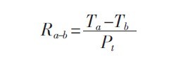
The thermal resistance R is the physical quantity for evaluating the thermal conductivity of the material. The thermal resistance Ra-b between the two points a and b is defined as [3]:
 (1)
(1)
Where Ta is the temperature of point a, the unit is °C, Tb is the temperature of point b, the unit is °C, Pt is the dissipated heat power, and the unit is W. As can be seen from equation (1), at the same heat dissipation power, if the thermal resistance between the two points is smaller, the temperature difference is smaller.
It is well known that there are three ways of heat transfer: conduction, convection, and radiation. The problems to be solved in the thermal management of LED lighting system mainly include how to transfer the heat generated by the chip to the surrounding heat dissipation structure by conduction, and then transfer the heat to the surrounding air through convection and radiation, and finally complete the whole heat dissipation process. . In this process, how to minimize the thermal resistance in the entire heat transfer channel is a core issue to improve the thermal performance of the entire system.
2 Thermal management optimization
2.1 Heat conduction and its optimization
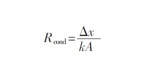
Thermal conduction is a heat transfer process that occurs directly in two directly contacting solids. The large amount of heat generated by the LED chip is first brought to the heat dissipation structure around the chip by heat conduction, so a good heat conductor is used to make the heat dissipation structure. The thermal conductivity k is used to measure the thermal conductivity of a material. The heat Qcond(W) transmitted by heat conduction is given by [4]:
 (2)
(2)
Where k is the thermal conductivity of the material, the unit is W/mK, A is the cross-sectional area of ​​the heat conductive material, the unit is m2, ΔT is the temperature difference between the two ends of the material, the unit is K, Δx is the distance of heat conduction, the unit is m. As can be seen from the formula (2), in order to improve the effect of heat conduction, the cross-sectional area of ​​the heat conductive material can be increased, the distance of heat conduction can be shortened, and a material having a high thermal conductivity can be used. On the other hand, because of the many interfaces in the thermal path in heat conduction, it is also important to use good thermal interface materials to improve the thermal conductivity of the interface.
In practical applications, the heat generated by the high-power LED chip is first transmitted through the LED chip package structure. How to establish a good heat conduction path between the LED chip and the outside world is very important. The traditional LED chip package is a formal installation method, which transfers the heat of the LED junction through the sapphire substrate, and the thermal conductivity of the sapphire substrate is only 42 W/mK, which is not conducive to the heat dissipation of the chip. Recently, flip-chip structures and vertical structure LED packages have been developed to improve heat transfer. The flip-chip LED is flip-chip mounted on a silicon substrate with a higher thermal conductivity (thermal conductivity of about 120 W/mK) by eutectic soldering technology [5], so that the heat generated by the LED can be quickly transmitted.
Come. The vertical structure LED transfers the GaN epitaxial layer to a substrate with high thermal conductivity such as silicon or copper by laser lift-off process [6], thereby greatly improving the heat dissipation effect. For the copper substrate, for example, the thermal conductivity of copper is 400 W/mK. about.
In the above-mentioned packaging methods such as dressing, vertical structure and flip-chip structure, the problem of how to fix the chip by using the thermal interface material is involved. In addition, a thermal interface material is required between the printed circuit board and the heat sink to fill the tiny air gap. Commonly used thermal interface materials include thermal conductive adhesives, phase change materials, thermally conductive elastomers, and low melting point alloys, such as conductive silver paste, thermal paste, eutectic solder alloy, and the like. Carbon nanotubes have very good thermal conductivity and their thermal conductivity is as high as 6 600 W/mK [7]. It can be used as a thermal interface material in future LED applications, but it has the disadvantages of complicated process and high cost.
2.2 Thermal convection and its optimization
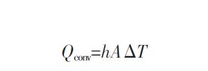
Thermal convection refers to the way heat is transferred away by the flow of liquid or gas. For LED lighting systems, the heat of the heat sink is usually dissipated into the surrounding air by means of thermal convection. Convection has two modes: natural convection and forced convection. The heat dissipation Qconv(W)[8] in the convection mode is given in the following equation:
 (3)
(3)
Where h is the heat transfer coefficient, the unit is W/m2K, A is the surface area of ​​the heat sink, the unit is m2, and ΔT is the temperature difference between the heat sink and the surrounding medium, and the unit is K. For different convection heat dissipation technologies, the heat transfer coefficient is very different. The heat transfer coefficient of forced water convection can be as high as 10 000 W/m2K, and the heat transfer coefficient of natural convection of air is generally considered to be about 10 W/m2K. In the use of the heat sink, the heat convection capability of the heat sink is closely related to the specific placement method.
In addition to natural convection and forced convection, heat pipe technology can also be used to improve the heat dissipation capacity of the system [9]. In some special applications, even water cooling can be used to achieve good heat dissipation. The choice of specific heat dissipation methods is not only related to the heat dissipation effect, but also depends on factors such as cost, reliability, and noise.
2.3 Thermal radiation and its optimization
Thermal radiation is the third way of heat transfer. All objects with temperatures above absolute zero can generate heat radiation. The higher the temperature, the greater the total energy radiated. The general heat radiation mainly depends on the visible light with longer wavelength. Infrared transmission.
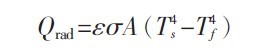
The heat Qrad(W) transmitted by thermal radiation is determined by the following equation [10]:
 (4)
(4)
Where ε is the emissivity of the surface of the object, dimensionless, σ is the Stephen-Boltzmann constant, the value is 5.67×10⁻⁸ W/m2K4, A is the area of ​​the heat-dissipating surface, the unit is m2, and Ts is the surface of the heat-dissipating material. Temperature, in K, Tf is the temperature of the fluid in the surrounding medium, usually the temperature of the surrounding air, in K. In other cases where the conditions are determined, the heat dissipation effect can be improved by increasing the emissivity of the surface of the heat sink. Taking an aluminum heat sink as an example, the surface treatment can be enhanced by using an anodizing process to improve the surface emissivity, thereby improving the heat dissipation effect [11]. For heat sink design, computational fluid dynamics can be used for simulation [12] to obtain more accurate design results and speed up the design process.
3 Thermal Management Design Example
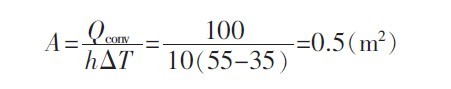
Assume that the LED lamp has a heat generation of 100 W, the LED heat sink base has a temperature of 55 ° C, and the ambient temperature is up to 35 ° C. According to formula (2), if the heat transfer coefficient of natural convection is 10 W/m2K, The area of ​​the heat sink base used should be: without considering heat radiation:
In order to ensure that the 1W LED chip used in the lighting fixture reaches a life of 50,000 hours, it is desirable to control the junction temperature of the LED chip to 90 °C, so the thermal resistance from the LED chip to the LED heat sink base cannot exceed (90-55)/1= 35 (°C/W). The thermal resistance is distributed as follows: the thermal resistance from the LED chip to the solder joint is 8 °C/W, and the thermal resistance of the solder joint to the heat sink base must be controlled at 27 °C/W, depending on the selected PCB board and thermal interface material. Parameters such as thermal conductivity k, thickness and area, using the following formula:
 (5)
(5)
To assess whether the thermal resistance on the heat transfer path can meet the design requirements.
4 Conclusion
In the thermal management design, first understand the thermal resistance of each link in the entire thermal path, draw a schematic diagram of the thermal resistance of the system, find the bottleneck of heat transfer, and then carry out key improvements. For example, in the selection of thermal interface materials, more attention should be paid to the selection of thermal interface materials with poor thermal conductivity. Under the premise of selecting the LED chip, the thermal management design uses the expected chip junction temperature and the working environment temperature as the two nodes of the design, allocates the temperature gradient budget on the thermal path between the two nodes, and estimates the corresponding thermal resistance value. The design should have sufficient margin to ensure that the junction temperature is within the expected range in a harsh environment, thus ensuring the long-term reliability of the LED chip. In each specific
In some designs, three heat transfer methods are used in combination. Take the design of the heat sink as an example. First, use a good conductor of heat to make full use of the heat conduction method. In addition, carefully design the shape of the heat sink according to the use environment to maximize the use of heat convection, and finally improve as much as possible. The emissivity of the surface of the heat sink is fully utilized to radiate heat.
It can be seen from the above analysis that the thermal management design of high-power LED lighting system is an engineering problem that needs to be considered comprehensively, and it must be optimized at the system level to achieve good heat dissipation.
Office Window Cleaning Robot apply to office, home, hotel, shop and so on. You can saves the labor, money, energy using smart window robot clean office. Office window robot is suitable for frame glass (rimless glass is also ok), door, wall. The noise is only 48dB when you use window robot clean office, giving you a quite environment.
Window Cleaning Robot Reviews beat HOBOT window robot, we become to Top sale . window cleaning robot test very good before leaving facotry. Welcome to place order ws - 960 window cleaning robot.

Specifications of robotic window cleaner:
Dimensions: 285*136*100mm
Weight: 0.92kg
Cleaning speed: 3′/㎡
Applicable Area: ≤100㎡
Working height: No limited
Anti-drop control: UPS / safety rope
Detection window frame: Auto recognition
Operation: Automatic / remote control
Alarm prompt function: Voice alarm
If there is anything confusing you, please feel free to contact me for further discussion. Our factory is in Shenzhen, China. Welcome to visit. It will be our honor to see you.
Office Window Cleaning Robot
Office Window Cleaning Robot,Building Window Cleaning Robot,Window Cleaning Robot Reviews,Office Building Window Cleaning Robot,Window Cleaning Robot Reviews,Window Cleaning Robot For Office
Zhengzhou Bangmi Smart Technology Co., Ltd. , https://www.globalcleanrobot.com