SMT production process
The basic process components of SMT include: silk screen (or dispensing), placement (curing), reflow soldering, cleaning, inspection, rework
1. Silk screen: Its function is to print solder paste or patch glue on the pad of PCB to prepare for soldering of components. The equipment used is a screen printing machine (screen printer), located at the forefront of the SMT production line.
2, dispensing: it is the glue to the fixed position of the PCB, its main role is to fix the components to the PCB. The equipment used is a dispenser, located at the forefront of the SMT line or behind the inspection equipment.
3. Mounting: Its function is to accurately mount the surface-assembled components to the fixed position of the PCB. The equipment used is a placement machine located behind the screen printing machine in the SMT production line.
4. Curing: The function is to melt the patch glue, so that the surface-assembled components and the PCB board are firmly bonded together. The equipment used is a curing oven located behind the placement machine in the SMT line.
5, reflow soldering: its role is to melt the solder paste, so that the surface assembly components and PCB board firmly bonded together. The equipment used is a reflow oven located behind the placement machine in the SMT line.
6. Cleaning: The function is to remove the welding residues (such as flux) which are harmful to the human body on the assembled PCB board. The equipment used is a washing machine, the position can be fixed, it can be online or not.
7. Detection: The function is to test the quality and assembly quality of the assembled PCB. The equipment used includes a magnifying glass, a microscope, an on-line tester (ICT), a flying probe tester, an automatic optical inspection (AOI), an X-RAY inspection system, and a function tester. The position can be configured in a suitable place on the production line according to the needs of the inspection.
8, repair: its role is to detect the failure of the PCB board rework. The tools used are soldering irons, rework stations, and the like. Configure anywhere in the production line.
First, single-sided assembly:
Incoming material inspection => silk screen solder paste (point patch adhesive) => patch => drying (curing) => reflow soldering => cleaning => detection => repair
Second, double-sided assembly:
A: incoming material inspection => PCB A-side silk screen solder paste (point patch adhesive) => patch => drying (curing) => A surface reflow soldering => cleaning => flap => PCB side B Screen printing solder paste (point patch adhesive) => patch => drying => reflow soldering (preferably only for side B => cleaning => detection => repair)
This process is suitable for use when a large SMD such as PLCC is attached to both sides of the PCB.
B: incoming material inspection => PCB A-side silk-screen solder paste (point patch adhesive) => patch => drying (curing) => A-side reflow soldering => cleaning => flap => PCB side B Point patch glue => patch => cure => B surface wave soldering => cleaning => detection => repair)
This process is suitable for reflow soldering on the A side of the PCB and B wave soldering on the B side. This process should be used in SMDs assembled on the B side of the PCB only when the SOT or SOIC (28) pins are below.
Third, single-sided mixing process:
Incoming material inspection => PCB A side silk screen solder paste (point patch glue) => patch => drying (curing) => reflow soldering => cleaning => plug-in => wave soldering => cleaning => detection = > Rework
Fourth, double-sided mixing process:
A: incoming material detection => PCB B-side point patch adhesive => patch => curing => flap => PCB A-side plug-in => wave soldering => cleaning => detection => repair
First post-inserted, suitable for SMD components more than separate components
B: incoming material detection => PCB A-side plug-in (pin bending) => flap => PCB B-side patch adhesive => patch => cure => flap => wave soldering => cleaning => Detection => Rework
Insert first and then paste, suitable for the case where the separation component is more than the SMD component
C: incoming material detection => PCB A side silk screen solder paste => patch => drying => reflow soldering => plug-in, pin bending => flap => PCB B-side patch adhesive => Patch => Cure => Flip => Wave Soldering => Cleaning => Detection => Rework A side mixing, B side mounting.
D: incoming material detection => PCB B-side point patch adhesive => patch => curing => flap => PCB A-side silk screen solder paste => patch => A-side reflow soldering => plug-in => B-side wave soldering => Cleaning => Detection => Rework A side mixing, B side mounting. First paste two sides SMD, reflow soldering, post-insertion, wave soldering E: incoming material detection => PCB B-side silk screen solder paste (point patch adhesive) => patch => drying (curing) => reflow soldering = > Flip => PCB A-side silk-screen solder paste => SMD => Drying = reflow soldering 1 (local soldering can be used) => Plug-in => Wave soldering 2 (if there are few plug-in components, manual soldering can be used) => Cleaning => Detection => Rework A side mount, B side mix.
Five, double-sided assembly process:
A: incoming material inspection, PCB A-side silk-screen solder paste (point paste), patch, drying (curing), A-side reflow soldering, cleaning, flipping; PCB B-side silk-screen solder paste (point patch) Glue), patch, dry, reflow soldering (preferably only for B side, cleaning, inspection, rework)
This process is suitable for use when a large SMD such as PLCC is attached to both sides of the PCB.
B: incoming material inspection, PCB A-side silk-screen solder paste (point paste), patch, drying (curing), A-side reflow soldering, cleaning, flipping; PCB B-side patch adhesive, patch , curing, B-side wave soldering, cleaning, inspection, rework) This process is suitable for reflow soldering on the A side of the PCB and B-side wave soldering. This process should be used in SMDs assembled on the B side of the PCB only when the SOT or SOIC (28) pins are below.
In the outdoor lighting section, the global urban transformation, urban construction, residential construction and road construction for market demand of high-power, high-brightness, energy-saving LED driver power supply is extremely large. Isolated Programmable LED Driver no need of Optocoupler and side current control circuit to realize isolating constant-current output. The circuit structure is very simple.


The advantage of MOSO isolated programmable Industrial Light LED Driver is small
input/output capacitance, small output wave, isolated output, high power
factor, high current precision and high reliability. Fixed output Industrial Light power supply has output open-circuit
protection, over-voltage protection and short-circuit protection.
Dimmable Industrial Light LED Driver built in 2-in-1 dimming and auto-react:0-10Vdc, PWM signal, dali control is optional.
Architecture and industrial Light LED Driver adopt Soft-switching patented technology, high efficiency up to 93%.
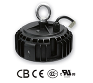
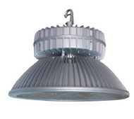
Programmable High Bay LED Driver
Programmable High Bay LED Driver, Isolated Programmable LED Driver,Programmable LED Driver,Programmable High Bay Light LED Driver
Moso Electronics , https://www.mosoleddriver.com