The MICRF009 is a single-chip SK/OOK (on-off key) RF receiver IC developed by Micrel Semiconductor. It has been enhanced in two main areas: improved sensitivity, reaching as low as 104dBm, and faster recovery time, typically up to 1ms. Like other QwikRadio products, the MICRF009 offers low power consumption and high integration, making it ideal for a wide range of wireless applications.
The MICRF009 supports two operational modes: fixed mode (FIX) and scan mode (SWP). In FIX mode, it functions as a conventional superheterodyne receiver, providing excellent selectivity and sensitivity. In SWP mode, it scans a broader RF spectrum using a patented scanning technique, which makes it suitable for use with low-cost, less accurate transmitters. This flexibility allows the device to adapt to different application scenarios effectively.
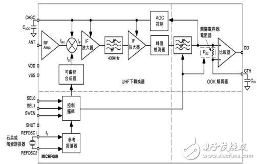
Figure 1. Block diagram of MICRF009
The MICRF009 integrates all post-detection (demodulator) data filtering, eliminating the need for an external baseband filter. Users can choose between two filter bandwidths by selecting the appropriate filter based on the data rate and modulation format. The IC operates in the frequency range of 300MHz to 440MHz, with a maximum data transmission rate of 2Kbps in fixed mode using Manchester encoding. Additionally, it features low RF retransmission radiation, ensuring efficient and clean signal processing.
As shown in Figure 1, the MICRF009 consists of three primary components: a UHF down-converter, an OOK demodulator, and a reference clock along with control logic. It also includes two capacitors (CTH, CAGC) and a timing component such as a quartz crystal or ceramic resonator. Alongside power coupling capacitors and the antenna impedance matching network, these are the only external components required to build a complete UHF receiver using the MICRF009. For optimal performance, it is recommended to match the MICRF009’s input impedance to the antenna, requiring just a few additional components for the matching network.
Designing a complete UHF receiver using the MICRF009 involves five basic steps: choosing the operating mode (fixed or scan), selecting the reference oscillator, setting the demodulator filter bandwidth, choosing the CTH capacitor, and selecting the CAGC capacitor.
1. Selecting the Operating Mode
(1) Fixed Mode
When the transmit frequency is precisely set, such as in systems using SAW or quartz crystal oscillators, the MICRF009 can be configured as a standard superheterodyne receiver. In this mode, the receiver is highly resistant to interference due to its narrow RF bandwidth. To activate fixed mode, connect the SWEN pin to ground.
(2) Scan Mode
When used with a low-cost LC transmitter, the MICRF009 should be configured in scan mode. In this mode, the local oscillator (LO) sweeps across a band wider than the data rate, effectively increasing the RF bandwidth. This allows the device to handle significant frequency offsets between the transmitter and receiver, even if the transmitter frequency drifts up to ±0.5%. In scan mode, approximately 1.5% of the band around the nominal transmit frequency can be captured, ensuring reliable operation without needing to adjust the receiver. The IF bandwidth remains at 680kHz regardless of the mode, maintaining consistent noise performance. However, the maximum data rate in scan mode is limited to about 1250Hz.
2. Selecting the Reference Oscillator
The MICRF009 uses an internal Colpitts reference oscillator for timing and tuning, controlled via the REFOSC pin. Three options are available: connecting a ceramic resonator, a quartz crystal, or driving the pin with an external signal. The reference frequency depends on the system’s transmit frequency and the selected mode (determined by the SWEN pin).
(1) Choosing Between Quartz Crystal and Ceramic Resonator
The IC already contains internal capacitors, so avoid using resonators with built-in capacitors. Use low ESR quartz crystals for better performance. In fixed mode, it's recommended to use a crystal, while in scan mode, either a crystal or ceramic resonator can be used. If an external signal is used, ensure it is AC-coupled and within the voltage range of 0.1VPP to 1.5VPP.
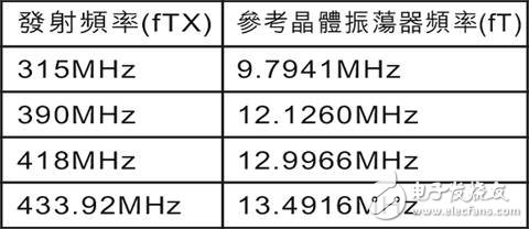
Table 1. Recommended reference crystal oscillator frequency for typical transmit frequency in fixed mode
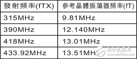
Table 2. Recommended reference crystal oscillator frequency for typical transmit frequency in scan mode
(2) Calculating the Reference Oscillator Frequency fT (Fixed Mode)
For any superheterodyne receiver, the difference between the local oscillator frequency (fLO) and the incoming transmit frequency (fTX) should equal the IF center frequency. The formula to calculate fLO is:
fLO = fTX ± 0.86(fTX / 315)
This gives two possible values for fLO, corresponding to high-end and low-end mixing. The reference oscillator frequency fT can then be calculated using:
fT = 2 × fLO / 64.5
This value is in MHz, and the REFOSC pin is connected to a quartz crystal with a frequency of fT, accurate to four decimal places. Table 1 provides examples of fT for common transmit frequencies in fixed mode.
(3) Calculating the Reference Oscillator Frequency fT (Scan Mode)
In scan mode, the calculation is simpler. The reference oscillator frequency fT is given by:
fT = 2 × fTX / 64.25
A precision of two decimal places is sufficient for fT in this mode. If the transmit frequency is particularly inaccurate, a quartz crystal may be necessary.
3. Selecting the CTH Capacitor
The DC level of the demodulated signal must be compressed using the external filter capacitor CTH and the on-chip switching capacitor resistance RSC. The selection of CTH depends on the data slice level time constant, which is influenced by factors like decoding response time and data encoding structure.
At 315MHz, the effective resistance of RSC is 145kΩ, which scales linearly with frequency. The formula for RSC at other frequencies is:
RSC = 145kΩ × 9.7940 / fT
It is recommended that the time constant Ï„ be 5 times the code rate. The effective impedance of the CTH pin is given by:
CTH = Ï„ / RSC
A ±20% X7R ceramic capacitor is usually sufficient for this purpose.
4. Selecting the CAGC Capacitor
The AGC (Automatic Gain Control) increases the dynamic range of the input signal. The rise time constant of the AGC signal is determined by the CAGC capacitor connected to the CAGC pin. To maximize the system range, the ripple of the AGC control voltage should be minimized. Ideally, the ripple should be less than 10 mVPP, so a capacitor larger than 0.47μF is recommended.
Careful management of the AGC control voltage allows the MICRF009 to operate in duty cycle mode. When the device is in power-down mode (SHUT pin high), the CAGC capacitor maintains a certain voltage. Upon resuming operation, only the voltage drop due to leakage needs to be replenished. For duty cycle operation, a low-leakage capacitor is recommended.
To further improve duty cycle performance, the AGC pull-up and pull-down currents must be activated immediately after the device exits power-down, typically within 10 ms. This helps reduce the time needed to recover the correct AGC voltage. The current amplification factor is 45.
(1) Selecting CAGC Capacitors in Continuous Mode
In continuous mode, a CAGC capacitor of 0.47μF to 4.7μF is generally recommended. If the capacitor is too large, the AGC response to the input signal may become too slow. The quiet time of the AGC (time to reach 0V) can be calculated using:
Δt = 1.333 × CAGC - 0.44
where CAGC is in μF and Δt is in seconds.
(2) Selecting CAGC Capacitors in Duty Cycle Mode
During power-down, the voltage drop of the CAGC capacitor must be quickly replenished upon restart. The MICRF009 pulls up or down the current by a factor of 45 after startup. This time is inversely proportional to the reference oscillator frequency fT. For example, when fT = 6.00 MHz, the time is 10.9 ms. Choosing the right CAGC capacitor and power-off duration ensures the voltage drop is restored within 10 ms.
However, the polarity of the voltage drop is unknown, meaning the AGC voltage could rise or fall. The worst-case scenario is when the voltage drop occurs at the recovery point, as the pull-up current is only 1/10 of the pull-down current. The voltage drop can be calculated using:
I / CAGC = ΔV / Δt
where I is the initial 10ms AGC pull-up current (67.5μA), CAGC is the capacitance of the AGC capacitor, Δt is the buck recovery time, and ΔV is the voltage drop. For example, with a 4.7μF CAGC capacitor and a 10ms recovery time, the allowable voltage drop is approximately 144mV.
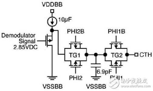
Figure 2. CTH pin interface circuit
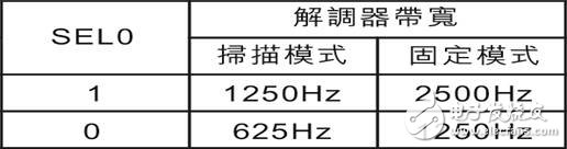
Table 3. 343.92MHz demodulator filter bandwidth and SEL0 relationship
5. Selecting the Demodulator Filter Bandwidth
The SEL0 pin controls the demodulator filter bandwidth in binary steps. In scan mode, the bandwidth ranges from 625 Hz to 1250 Hz, while in fixed mode, it ranges from 1250 Hz to 2500 Hz, as shown in Table 3. By default, SEL1 is connected to VSS. Note that the values in Table 1 are theoretical, and the actual filter bandwidth depends on the operating frequency.
(1) Power Supply Bypass Capacitor
It is highly recommended to use a power supply bypass capacitor, connected between VDDBB and VDDRF with as short leads as possible. For best results, connect VSSRF to VSSBB and VDDBB to VDDRF, allowing the bandpass current to flow through the RF return path.
(2) Improving Selectivity by Optimizing the Bandpass Filter
In a noisy environment, a fixed bandpass network can be added between the ANT pin and the VSSRF pin to enhance receiver selectivity and provide input overload protection. The minimum input configuration is shown in Figure 9, offering some filtering and necessary protection against overloading.
(3) Reducing Output Noise
During quiescence (no signal), the output data (DO pin) may randomly fluctuate due to noise. Most decoders can distinguish between random noise and actual data. However, there are three ways to reduce output noise: analog suppression, digital suppression, and filtering high-frequency noise. The simplest solution is to add a small amount of analog suppression to the CTH pin to prevent the internal comparator from being triggered by noise.
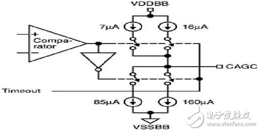
Figure 3. CAGC pin interface circuit
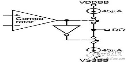
Figure 4. DO pin interface circuit
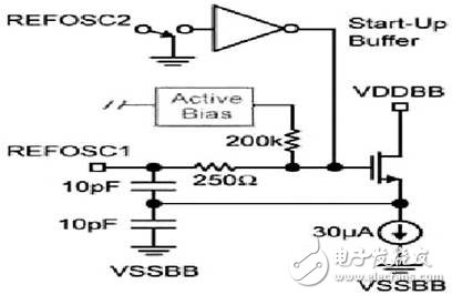
Figure 5. REFOSC pin interface circuit
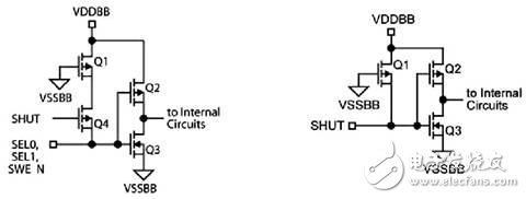
Figure 6. SEL0/SEL1/SWEN pin (6a), and SHUT pin (Figure 6b) interface circuit
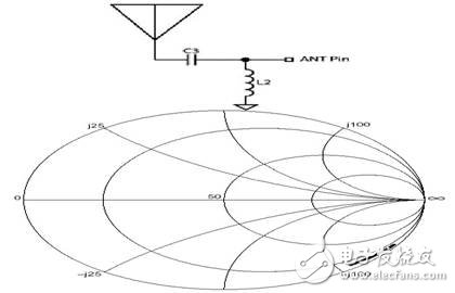
Figure 7. Antenna input impedance matching IC input impedance
Typically, a 20mV to 30mV signal is sufficient. This can be achieved by connecting a mega-ohm resistor between the CTH pin and VSSBB or VDDBB. The specific value depends on the desired offset polarity. Since the AGC noise at the internal comparator output is always the same (set by the AGC), the deviation suppression requirement changes with the noise intensity. Introducing a small amount of suppression is enough to keep the output quiet. Typical suppression resistors range from 10M to 6.8M ohms.
6. I/O Pin Interface Circuit
The interface circuits for the various I/O pins of the MICRF009 are shown in Figures 2–8. For brevity, ESD protection circuits are not labeled in the figures.
7. Antenna Impedance Matching
Matching the antenna input impedance to the IC input impedance is critical. As shown in Figures 7 and 4, the antenna input impedance is frequency-dependent. The ANT pin can be matched to 50 ohms using an L-shaped network, as illustrated in Figure 3. This involves a shunt inductor between the antenna input and ground, and another component in series between the antenna input and the ANT pin.
The inductor values depend on the PCB material, thickness, grounding configuration, and wiring path length. The values provided in Table 4 assume a PCB thickness of 0.031", FR4 board, rigid board, grounded bottom layer, and short wiring paths. The inductors used are wire-wound 0063 or 0805 surface mount inductors from MuRata and Coilcraft. Any brand of high SRF wirewound inductors can also be used.
Third, Application Examples
Figure 8 shows a typical application of the MICRF009 UHF receiver IC, operating continuously in scan mode at a typical frequency of 315 MHz. The frequency reference (Y1) can be customized, and the antenna length can be adjusted accordingly. If an alternative input filter is used, the capacitance of C4 will also change. If the data rate changes by 1 kbps, the resistance of R1 must also be adjusted. The bill of materials for the application example is shown in Table 5. Figure 9 displays the corresponding PCB layout.
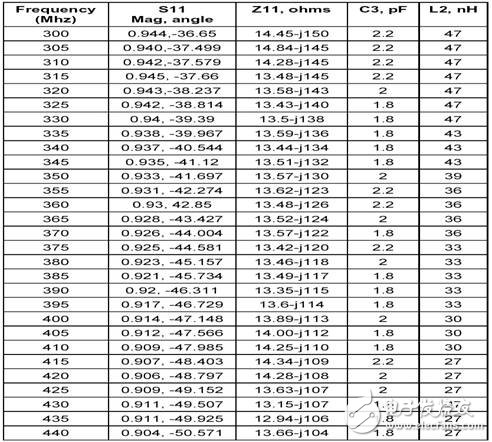
Table 4. Technical parameters of the shunt inductor for matching
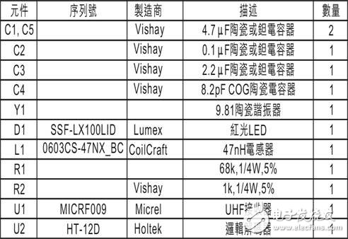
Table 5. Bill of materials for the application example
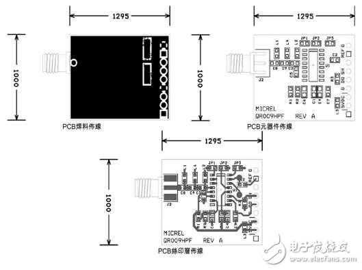
Figure 9. Minimum input configuration to improve selectivity by optimizing the bandpass filter
Outdoor Rental LED Display is hot selling product in the led screen market. We usually use Nova MSD300 sending card and MRV328 receving card, other controll system also can be accepted, like Linsin,colorlight and so on.....About the led lamp, we use kinglight led lamp, IC is ICN2038S, refresh rate is 1920hz. We also provide other option if the client need higher quality, like Nationstar led lamp and refresh rate can make 3840hz. This 500x500mm LED display panel can also can make curved led display, ±15° flexible curved option.
Application:
* Business Organizations:
Supermarket, large-scale shopping malls, star-rated hotels, travel agencies
* Financial Organizations:
Banks, insurance companies, post offices, hospital, schools
* Public Places:
Subway, airports, stations, parks, exhibition halls, stadiums, museums, commercial buildings, meeting rooms
* Entertainments:
Movie theaters, clubs, stages.
Outdoor Rental LED Display,P3.91 Led Display,Led Advertising Display,Led Display Panel
Guangzhou Chengwen Photoelectric Technology co.,ltd , https://www.cwleddisplay.com