Abstract: DS28DG02 is a 2kb SPI ™ EEPROM with PIO, real-time clock (RTC), reset, battery monitor and watchdog, which combines multiple functions required in portable devices and embedded applications. This application note supplements the product data sheet, gives detailed information on the SPI interface and its write protection scheme, and explains how to use the device ’s 12 PIO and RTC alarm clock functions. The documentation also includes battery selection guides, RTC crystal pad shielding, and software response to alarm events.
The communication interface DS28DG02 is a slave EEPROM device. The host usually composed of a microcontroller uses it to access its resources through a serial peripheral interface (SPI). SPI was originally established by Motorola for the MC68HCxx series of microcontrollers. Table 1 lists the standard SPI signal names and their functions.
Table 1. SPI signal names
Basic SPI communication uses shift registers in both the master and slave. The input and output of the shift register are connected to form a loopback, as shown in Figure 1. Driven by the master, the clock signal transfers the 8-bit serial data block from the master to the slave, and at the same time from the slave to the master, thereby implementing the SPI full-duplex protocol. However, most SPI slaves, including DS28DG02, need a command before receiving or sending data. Similarly, in half-duplex mode, data is transferred from the master to the slave or from the slave to the master.
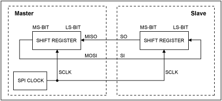
Figure 1. SPI communication concept
The SPI specification defines four modes, selected by the control bits CPOL and CPHA in the SPI host. There is no standard on how to refer to these modes. Table 2 lists the commonly used mode definitions in the SPI documentation.
Table 2. SPI mode definition
DS28DG02 supports SPI mode (0,0) and (1,1). In these modes, the data is collected (synchronous input) on the rising edge of the clock, and the output is shifted (may change) on the falling edge of the clock. The clock state of the CSZ falling edge tells the DS28DG02 which SPI mode the host is using. If you try to communicate in mode (1,0) or (0,1), you cannot determine the behavior of the device.
For other information about the SPI protocol and timing, please refer to the SPI interface section in the DS28DG02 data sheet. You can also search for the keyword "SPI slave TIming" on the Internet. Most of the documents searched through the network are about microcontrollers. According to the internal register settings, these microcontrollers can implement SPI master or slave. Third-party documents provide a good introduction to the SPI concept and explain the settings of the SPI host. These documents are:
http: // (general information)
http: // (Host Settings)
Write protection scheme The SPI memory uses a 3-level scheme to protect the memory from unintentional or unauthorized changes: the WEN bit in the SPI status register; the block write protection using the control bits in the SPI status register; the pin status and SPI status Hardware write protection of the enable bit in the register. DS28DG02's unique register write protection and block write protection are on the same level, but use different memory areas. Table 3 lists the control bits and their effect on the memory.
Table 3. Write protection control
Level 1: The WEN bit in the SPI status register is powered on, after successfully completing the write function command, or through the SPI command WRDI (write disable), this bit is cleared. The only way to set the WEN bit is through the SPI command WREN (write enable). Note: When the SPI host fails, the WEN bit can prevent the writeable memory from failing.
Level 2: The BP1: BP0 bits in the SPI status register, a commonly used write protection method, uses the two nonvolatile bits of the SPI status register (BP1: BP0) for all bits, upper half, and upper quarter of the EEPROM It is partially write-protected or not. The control bit is in the SPI status register and can be protected by hardware write protection. When there is no hardware write protection, the block write protection can be modified through software control. Note: Block write protection configures some EEPROMs as read-only, while leaving other EEPROMs to the host to store data, which can be modified when the final product is working normally.
Level 2: RPROT bit in the SPI status register This is a special function of the DS28DG02. This method uses the non-volatile RPROT bit in the SPI status register to write-protect user-writable bytes at addresses 120h and higher. If RPROT is 1, write-protect these addresses. This protects the RTC, RTC alarm register, multi-function control / setting register, and alarm / status register to prevent write operations to the PIO. This level of write protection does not protect the power-on default values ​​of PIO-related registers. These values ​​are stored in 10Ah to 10Fh. The RPROT bit is in the SPI status register and can be protected by hardware write protection. When there is no hardware write protection, RPROT can be modified through software control. Note: Register write protection prevents accidental changes to RTC and its alarms, as well as changes to the registers that define the DS28DG02 function in the final product (eg, watchdog, battery monitor, RTC).
Level 3: WPEN bit in the SPI status register This method uses the WPZ pin and the WPEN bit in the SPI status register. This function only protects the non-volatile bits of the SPI status register, especially the block protection bits BP1: BP0, RPROT and WPEN. When the WPEN bit is set to 1, the WPZ pin is enabled to control all nonvolatile bits in the SPI status register, including WPEN. For the factory SPI memory, the WPEN bit reads 0. In this way, even if the WPZ pin is connected to ground, the memory on the circuit board tester can be programmed. In the last step, after programming the memory, the tester sets level 2 protection and writes the WPEN bit to 1 to activate the hardware write protection. As long as the logic state of the WPZ pin remains at 0, the non-volatile bits of the SPI status register will remain write-protected. To modify any non-volatile bit, you must change the logic state of the WPZ pin to 1, for example, by temporarily connecting the pin to VCC via a jumper. Note: The hardware write protection permanently sets the level 2 protection, but there is still a back door (WPZ pin) for future corrections.
Note: After the register write protection is permanently enabled, the only way to clear the watchdog, RTC and battery alarms is to power on VCC again. Regardless of the VCC power supply, after replacing the battery, clear the multi-function control / setting register and RTC and its alarm register. If both hardware write protection and register write protection are activated (RPROT = 1, WPEN = 1, WPZ pin is connected to ground GND), the user may need to call the device manufacturer to reconfigure the device and run it again.
Battery selection The DS28DG02 requires a battery to maintain the configuration information stored in the address 134h multifunction control / setting register and keep the RTC running. If VCC can be used permanently, no battery is needed and the VBAT pin is connected to VCC. If VCC is interrupted and there is no battery backup, all bits are 0 when the multi-function control / setting register is powered on. This will stop the RTC and disable the clock alarm, watchdog and battery monitor. This is a normal setting and has nothing to do with applications that do not use RTC and watchdog. Typical DS28DG02 applications will use at least RTC or watchdog, so a battery is required and the battery is monitored.
Only cut off VCC, can save battery power consumption. There are two situations to note: a) when the RTC oscillator is stopped (off, OSCE = 0); b) when the RTC oscillator is turned on (running, OSCE = 1). In theory, there is a third situation related to the battery monitor. However, the maximum load of the battery monitor (IMAX = 20µA) lasts only 2 seconds per hour. Therefore, the average load current is 11nA (20µA x 2/3600), which is two times lower than the load when the RTC is turned off. The battery monitor does not shorten the battery life, because the monitoring is only performed when the VCC is working, and the RTC and other non-volatile memory cells are powered by the VCC, not the battery.
The typical battery voltage of DS28DG02 is 3V, which is powered by one lithium battery (Li +) or two silver oxide button batteries connected in series. The capacity of these batteries is usually expressed in mAh (milliampere hours). Through load resistance, measuring the time when the battery voltage drops to the specified threshold to obtain performance indicators, the method is similar to some applications. The battery manufacturer's data sheet has detailed information:
http: //
http: //
http://data.energizer.com/DataSheets.aspx
Assuming that the battery is similar to the capacitor, the discharge time of the battery is t = Q / I. For example, if the battery is 1mAh and the discharge current is 1µA, then the discharge time is:

According to the following formula, this result is multiplied by the ratio of battery capacity and discharge current:

For example, if the load current is 10µA, a 48mAh battery can run the RTC 48/10 x 41.66, or 200 days. At around + 25 ° C, the maximum load current when RTC is on is 4.7µA. Therefore, the same battery can be used continuously:

Two batteries in series can double the voltage and capacity, but does not extend the battery life. To determine the time of use, the capacity of one battery must be brought to Equation 2, because current flows through each battery in series and discharges each battery at the same rate.
There are 12 PIO channels using PIODS28DG02. In typical applications, some PIOs are used as inputs, others are used as outputs, and some are not used at all. PIOs (PIO0 to PIO7, PIO8 to PIO11) that are "close" on the memory map are not close on the circuit board. For TSSOP, all even PIOs are on the left side of the package, and odd PIOs are on the right side of the package. For TQFN, 3 even PIOs are located on the west side of the package, 3 odd PIOs are located on the east side of the package, and the remaining 6 PIOs, including odd and even numbers, are located on the south side of the package. Although this looks unusual, it does not affect the use of the device.
If there is no PIO in the output mode that needs to sink or source a large current, the small current output mode can be used. In the low current output mode, for all PIOs sharing the same memory address, PIO read and write are performed simultaneously. If the 5th to 8th PIOs need to be read or written at the same time, select PIO channel 0 to channel 7 and assign them to the nodes in the application in the most suitable way for the board layout topology. Because the high-current mode writing is not performed at the same time, only PIO is used when optimizing the layout of the circuit board. The following example describes a method of allocating PIO channels.
Configuration example
Looking at the PIO pin assignment of the DS28DG02 in a counter-clockwise direction, the PIO sequence sharing the same memory address is 0, 4, 6, 2, 3, 7, 5, 1. This order is independent of package type. Obviously close together are the 6th, 2nd, 3rd and 7th channels. For the other two outputs, channel 0 and channel 4 are assigned to them because the pins are close. This method does not use channels 1 and 5. The output type is set in groups of 4 PIOs, 0 to 3, 4 to 7, and 8 to 11; PIOs in the same group have the same output type. The four outputs in the example require push-pull. For the distribution just made, this can be channels 0 to 3, or channels 4 to 7. Since the first channel is not used, only the 0th, 2nd and 3rd channels, therefore, this output type cannot be satisfied.
To meet the requirements of the output type, the channel assignment must be changed. Channels 4 to 7 are now used for push-pull (arbitrarily selected), and channels 2 and 3 are open drain. In this way, the 0th and 1st channels are not used. The inputs are assigned to channels 8 to 11 and they also share the same memory address.
Next, you must define the power-on default register value for this configuration and write to the corresponding memory address. The following table uses the following colors to explain the choices made.
PIO output state power-on default
Note: In this example, assume that the application requires channels 2 to 5 to be powered on with logic 1, and channels 6 and 7 to be powered on with logic 0.
Power-on default value in PIO direction
Power-on default value for PIO reverse read (PIO0 to PIO7)
PIO reverse read power-on defaults (PIO8 to PIO11), PIO output type and output mode
Using the communication instance definition in the data, update the PIO defined as output in the following sequence:
To generate a waveform pattern in PIO, it is not necessary to repeat the entire sequence with different PIO data. Instead, send the required PIO data bytes; the first, third, and fifth bytes are used to update the PIO. Since PIO 8 to 11 are assigned as inputs, the other bytes (2nd, 4th, and 6th bytes, etc.) have no effect.
The following sequence reads the PIO defined as input:
To quickly read from the PIO repeatedly, it is not necessary to repeat the entire sequence. Instead, use the starting address 126h to read the required bytes. The 1st, 3rd and 5th bytes return the channel status defined as output. The other bytes (2nd, 4th, and 6th bytes, etc.) report the data assigned to input PIO 8 to 11.
PIO high current mode For write operations, PIO can work in low current mode or high current mode. Select the mode for all PIO lines in the same way. In the low current mode, all PIOs sharing the same byte address switch simultaneously. In addition, if access to the PIO is started with the write address 120h, for each data byte received by the DS28DG02, the write address switches between 120h (PIO0 to PIO7) and 121h (PIO8 to PIO11). This method supports fast writing to the PIO, so there is no need to execute the WREN command before the next write access.
In high-current and low-current modes, PIO has the same current sink or source capability. However, in high current mode (OTM = 1), PIO switches continuously one channel at a time; the PIO current slew rate is limited by the active circuit. High current mode does not use address switching. The address is incremented from 120h to 121h, then 122h, and so on. To write to address 120h again, a new write sequence is required.
If the DS28DG02 has a stable VCC power supply, a reset is generated immediately after the PIO is turned on, and the induced voltage spike enters the VCC monitor and is mistaken for a power failure. In this case, either the high current mode must be used, or the number of channels that are switched at a time is less than 8, and the high current mode is simulated by software to ensure that the current change will not exceed the maximum rated ± 50mA.
Various package types and sizes of RTC crystal and PCB layout provide 32kHz table crystal. The PCB layout in the DS28DG02 data sheet assumes that the crystal pitch and the package (TSSOP—0.65mm; TQFN—0.50mm) pin pitch match. This is a very tight pitch, and it may not be easy to obtain such a small crystal. In order to adapt to a larger crystal, the PCB layout needs to be modified, as shown in Figure 2. It is important to maintain a protective ring and local ground plane. The traces from the crystal pins X1 and X2 to the crystal pad should be as symmetrical as possible.
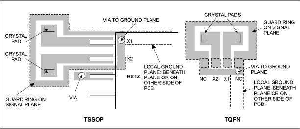
Figure 2. Alternative PCB layout
For detailed information on crystal selection, please refer to Maxim Application Note # 616, Considerations for Maxim Real-Time Clock Crystal Selection. The document also includes the technical data of the SMD crystal, as well as links to other supplier websites.
Clock alarm DS28DG02 can generate RTC alarms from once per second to once per month. The alarm is issued through the ALMZ pin, which is also used by the battery alarm and watchdog alarm. As a prerequisite for the clock alarm, RTC must be running and the clock alarm must be enabled (OSCE = 1, CAE = 1).
Generally speaking, to eliminate the clock alarm, the clock state must match the value in the alarm register. There are 4 RTC alarm clock registers: seconds, minutes, hours, day of the week or month of the month. The most significant bits in the alarm register are AM1 to AM4, and they control whether the register participates in the comparison. The DY / DT bit at address 133h specifies whether the remaining 6 bits are compared with the RTC's day of the week or month of the month. In other respects, the bit allocation of the alarm register and RTC match.
After defining the alarm time and frequency, write each bit (BCD code) to the template and convert the result to hexadecimal format ("Hex" column) to generate clock alarm register data. Then, through the SPI write sequence, write the obtained data into the alarm register. The following example explains this process. The color representation here is the same as the PIO section above.
Example 1: An alarm clock is generated every 25 minutes and 30 seconds
Note: For generating alarms every hour, every minute, or every second, 12/24 bits (the 6th bit of addresses 132h and 12Bh) are not used. To generate an alarm at 30 seconds per minute, change the 7th bit of address 131h to 1. This does not include minutes from comparison.
Example 2: 24-hour format, alarm clock is generated every day at 22:59:59
Example 3: 12-hour format, an alarm is generated at 6:30:00 PM on the first day of each week
Note: The day of the week counters use codes 1 to 7. The counter value of the day of the week can be arbitrarily assigned. 1Generally assigned to Sunday (US standard), but also assigned to Monday (European standard).
Watchdog CPU monitoring circuit generally uses watchdog. Technically, the watchdog can be interpreted as a re-triggerable monostable mode of operation. In an unstable state, the microcontroller periodically adds a positive pulse to the watchdog's trigger input WDI to maintain a single-shot trigger. If the microcontroller cannot do this, the watchdog times out and resets the microcontroller.
Select the watchdog timeout of DS28DG02 through the WD1: WD0 bits of the SPI status register. When the write access to the register is not blocked (RPROT = 0), write 1 to the WDE bit at address 134h to activate the watchdog. When the watchdog stops working, the alarm at address 135h and the WDA bit of the status register are set; the WDOZ pin (default) or ALMZ pin (another option) shared by the clock alarm and battery monitor, and the RSTZ pin go low Flat state.
The watchdog is disabled when the battery is installed (battery installation) or power-on reset (if there is no battery) (WDE = 0). Write 1 to the WDE bit. After the watchdog is activated, even if VCC is cut off, the watchdog can keep working through the battery backup power supply. When VCC increases, or the WDE bit is set, the internal counter of the watchdog is cleared, so that the microcontroller has time to complete its power-up before the watchdog needs to be re-triggered.
Alarm response There are 6 bits left in the DS28DG02 alarm and status register at address 135h to indicate important events. When such an event occurs, the microcontroller should treat it specially and respond separately, as shown below. If RPROT = 0, write 0 to this register and all alarms will be cleared.
Conclusion DS28DG02 is a very flexible and easy-to-use component in portable devices and other applications that require CPU monitoring functions such as memory, RTC, PIO, and power monitor and watchdog.
The communication interface DS28DG02 is a slave EEPROM device. The host usually composed of a microcontroller uses it to access its resources through a serial peripheral interface (SPI). SPI was originally established by Motorola for the MC68HCxx series of microcontrollers. Table 1 lists the standard SPI signal names and their functions.
Table 1. SPI signal names
| Motorola name | Features | Other names |
| SCLK | Serial clock, push-pull drive, generated by the host. If the rise time and fall time specifications are met, an open-drain drive can be used. | SCK, SK, C |
| MISO | Data line from slave to master, "master input, slave output". The high-impedance push-pull output driven by the slave is connected to the serial input of the master. | SO, DO, Q |
| MOSI | Data line from master to slave, "master output, slave input". The high-impedance push-pull output driven by the master is connected to the serial input of the slave. | SI, DI, D |
| Active low SS | Slave selection, push-pull output, generated by the master. | CSZ, active low CS |
Basic SPI communication uses shift registers in both the master and slave. The input and output of the shift register are connected to form a loopback, as shown in Figure 1. Driven by the master, the clock signal transfers the 8-bit serial data block from the master to the slave, and at the same time from the slave to the master, thereby implementing the SPI full-duplex protocol. However, most SPI slaves, including DS28DG02, need a command before receiving or sending data. Similarly, in half-duplex mode, data is transferred from the master to the slave or from the slave to the master.
Figure 1. SPI communication concept
The SPI specification defines four modes, selected by the control bits CPOL and CPHA in the SPI host. There is no standard on how to refer to these modes. Table 2 lists the commonly used mode definitions in the SPI documentation.
Table 2. SPI mode definition
| SPI mode | CPOL | CPHA | Explanation |
| 0 or (0,0) | 0 | 0 | The clock idle state is low. Collect data on the rising edge of the clock and shift the output on the falling edge of the clock. |
| 1 or (0,1) | 0 | 1 | The clock idle state is low. Collect data on the falling edge of the clock and shift the output on the rising edge of the clock. |
| 2 or (1,0) | 1 | 0 | The clock idle state is high. Collect data on the falling edge of the clock and shift the output on the rising edge of the clock. |
| 3 or (1,1) | 1 | 1 | The clock idle state is high. Collect data on the rising edge of the clock and shift the output on the falling edge of the clock. |
DS28DG02 supports SPI mode (0,0) and (1,1). In these modes, the data is collected (synchronous input) on the rising edge of the clock, and the output is shifted (may change) on the falling edge of the clock. The clock state of the CSZ falling edge tells the DS28DG02 which SPI mode the host is using. If you try to communicate in mode (1,0) or (0,1), you cannot determine the behavior of the device.
For other information about the SPI protocol and timing, please refer to the SPI interface section in the DS28DG02 data sheet. You can also search for the keyword "SPI slave TIming" on the Internet. Most of the documents searched through the network are about microcontrollers. According to the internal register settings, these microcontrollers can implement SPI master or slave. Third-party documents provide a good introduction to the SPI concept and explain the settings of the SPI host. These documents are:
http: // (general information)
http: // (Host Settings)
Write protection scheme The SPI memory uses a 3-level scheme to protect the memory from unintentional or unauthorized changes: the WEN bit in the SPI status register; the block write protection using the control bits in the SPI status register; the pin status and SPI status Hardware write protection of the enable bit in the register. DS28DG02's unique register write protection and block write protection are on the same level, but use different memory areas. Table 3 lists the control bits and their effect on the memory.
Table 3. Write protection control
| level | Control bit | Protected memory |
| 1 | WEN | All writable memory addresses and SPI status registers |
| 2 | BP1: BP0 | Address 000h to 0FFh |
| 2 | RPROT | Address 120h to 135h |
| 3 | WPEN (combined with WPZ pin status) | SPI status register, only non-volatile bits. |
Level 1: The WEN bit in the SPI status register is powered on, after successfully completing the write function command, or through the SPI command WRDI (write disable), this bit is cleared. The only way to set the WEN bit is through the SPI command WREN (write enable). Note: When the SPI host fails, the WEN bit can prevent the writeable memory from failing.
Level 2: The BP1: BP0 bits in the SPI status register, a commonly used write protection method, uses the two nonvolatile bits of the SPI status register (BP1: BP0) for all bits, upper half, and upper quarter of the EEPROM It is partially write-protected or not. The control bit is in the SPI status register and can be protected by hardware write protection. When there is no hardware write protection, the block write protection can be modified through software control. Note: Block write protection configures some EEPROMs as read-only, while leaving other EEPROMs to the host to store data, which can be modified when the final product is working normally.
Level 2: RPROT bit in the SPI status register This is a special function of the DS28DG02. This method uses the non-volatile RPROT bit in the SPI status register to write-protect user-writable bytes at addresses 120h and higher. If RPROT is 1, write-protect these addresses. This protects the RTC, RTC alarm register, multi-function control / setting register, and alarm / status register to prevent write operations to the PIO. This level of write protection does not protect the power-on default values ​​of PIO-related registers. These values ​​are stored in 10Ah to 10Fh. The RPROT bit is in the SPI status register and can be protected by hardware write protection. When there is no hardware write protection, RPROT can be modified through software control. Note: Register write protection prevents accidental changes to RTC and its alarms, as well as changes to the registers that define the DS28DG02 function in the final product (eg, watchdog, battery monitor, RTC).
Level 3: WPEN bit in the SPI status register This method uses the WPZ pin and the WPEN bit in the SPI status register. This function only protects the non-volatile bits of the SPI status register, especially the block protection bits BP1: BP0, RPROT and WPEN. When the WPEN bit is set to 1, the WPZ pin is enabled to control all nonvolatile bits in the SPI status register, including WPEN. For the factory SPI memory, the WPEN bit reads 0. In this way, even if the WPZ pin is connected to ground, the memory on the circuit board tester can be programmed. In the last step, after programming the memory, the tester sets level 2 protection and writes the WPEN bit to 1 to activate the hardware write protection. As long as the logic state of the WPZ pin remains at 0, the non-volatile bits of the SPI status register will remain write-protected. To modify any non-volatile bit, you must change the logic state of the WPZ pin to 1, for example, by temporarily connecting the pin to VCC via a jumper. Note: The hardware write protection permanently sets the level 2 protection, but there is still a back door (WPZ pin) for future corrections.
Note: After the register write protection is permanently enabled, the only way to clear the watchdog, RTC and battery alarms is to power on VCC again. Regardless of the VCC power supply, after replacing the battery, clear the multi-function control / setting register and RTC and its alarm register. If both hardware write protection and register write protection are activated (RPROT = 1, WPEN = 1, WPZ pin is connected to ground GND), the user may need to call the device manufacturer to reconfigure the device and run it again.
Battery selection The DS28DG02 requires a battery to maintain the configuration information stored in the address 134h multifunction control / setting register and keep the RTC running. If VCC can be used permanently, no battery is needed and the VBAT pin is connected to VCC. If VCC is interrupted and there is no battery backup, all bits are 0 when the multi-function control / setting register is powered on. This will stop the RTC and disable the clock alarm, watchdog and battery monitor. This is a normal setting and has nothing to do with applications that do not use RTC and watchdog. Typical DS28DG02 applications will use at least RTC or watchdog, so a battery is required and the battery is monitored.
Only cut off VCC, can save battery power consumption. There are two situations to note: a) when the RTC oscillator is stopped (off, OSCE = 0); b) when the RTC oscillator is turned on (running, OSCE = 1). In theory, there is a third situation related to the battery monitor. However, the maximum load of the battery monitor (IMAX = 20µA) lasts only 2 seconds per hour. Therefore, the average load current is 11nA (20µA x 2/3600), which is two times lower than the load when the RTC is turned off. The battery monitor does not shorten the battery life, because the monitoring is only performed when the VCC is working, and the RTC and other non-volatile memory cells are powered by the VCC, not the battery.
The typical battery voltage of DS28DG02 is 3V, which is powered by one lithium battery (Li +) or two silver oxide button batteries connected in series. The capacity of these batteries is usually expressed in mAh (milliampere hours). Through load resistance, measuring the time when the battery voltage drops to the specified threshold to obtain performance indicators, the method is similar to some applications. The battery manufacturer's data sheet has detailed information:
http: //
http: //
http://data.energizer.com/DataSheets.aspx
Assuming that the battery is similar to the capacitor, the discharge time of the battery is t = Q / I. For example, if the battery is 1mAh and the discharge current is 1µA, then the discharge time is:
According to the following formula, this result is multiplied by the ratio of battery capacity and discharge current:
For example, if the load current is 10µA, a 48mAh battery can run the RTC 48/10 x 41.66, or 200 days. At around + 25 ° C, the maximum load current when RTC is on is 4.7µA. Therefore, the same battery can be used continuously:
Two batteries in series can double the voltage and capacity, but does not extend the battery life. To determine the time of use, the capacity of one battery must be brought to Equation 2, because current flows through each battery in series and discharges each battery at the same rate.
There are 12 PIO channels using PIODS28DG02. In typical applications, some PIOs are used as inputs, others are used as outputs, and some are not used at all. PIOs (PIO0 to PIO7, PIO8 to PIO11) that are "close" on the memory map are not close on the circuit board. For TSSOP, all even PIOs are on the left side of the package, and odd PIOs are on the right side of the package. For TQFN, 3 even PIOs are located on the west side of the package, 3 odd PIOs are located on the east side of the package, and the remaining 6 PIOs, including odd and even numbers, are located on the south side of the package. Although this looks unusual, it does not affect the use of the device.
If there is no PIO in the output mode that needs to sink or source a large current, the small current output mode can be used. In the low current output mode, for all PIOs sharing the same memory address, PIO read and write are performed simultaneously. If the 5th to 8th PIOs need to be read or written at the same time, select PIO channel 0 to channel 7 and assign them to the nodes in the application in the most suitable way for the board layout topology. Because the high-current mode writing is not performed at the same time, only PIO is used when optimizing the layout of the circuit board. The following example describes a method of allocating PIO channels.
Configuration example
| Output: | 6 |
| Output type: | 4 way push-pull, 2 way open drain |
| Output mode: | Small current (simultaneous writing) |
| Enter: | 4 |
| Read backward | no |
| did not use: | 2 PIO |
Looking at the PIO pin assignment of the DS28DG02 in a counter-clockwise direction, the PIO sequence sharing the same memory address is 0, 4, 6, 2, 3, 7, 5, 1. This order is independent of package type. Obviously close together are the 6th, 2nd, 3rd and 7th channels. For the other two outputs, channel 0 and channel 4 are assigned to them because the pins are close. This method does not use channels 1 and 5. The output type is set in groups of 4 PIOs, 0 to 3, 4 to 7, and 8 to 11; PIOs in the same group have the same output type. The four outputs in the example require push-pull. For the distribution just made, this can be channels 0 to 3, or channels 4 to 7. Since the first channel is not used, only the 0th, 2nd and 3rd channels, therefore, this output type cannot be satisfied.
To meet the requirements of the output type, the channel assignment must be changed. Channels 4 to 7 are now used for push-pull (arbitrarily selected), and channels 2 and 3 are open drain. In this way, the 0th and 1st channels are not used. The inputs are assigned to channels 8 to 11 and they also share the same memory address.
Next, you must define the power-on default register value for this configuration and write to the corresponding memory address. The following table uses the following colors to explain the choices made.
| Value resulTIng from configuraTIon / applicaTIon requirements | |
| Arbitrary assignment, "don't care" condition | |
| (Not assigned, reserved) |
PIO output state power-on default
| ADDR | b7 | b6 | b5 | b4 | b3 | b2 | b1 | b0 | Hex | |
| 10Ah | 0 | 0 | 1 | 1 | 1 | 1 | 0 | 0 | 3C | |
| 10Bh | 0 | 0 | 0 | 0 | 0 | 0 | 0 | 0 | 00 |
Power-on default value in PIO direction
| ADDR | b7 | b6 | b5 | b4 | b3 | b2 | b1 | b0 | Hex | |
| 10Ch | 0 | 0 | 0 | 0 | 0 | 0 | 1 | 1 | 03 | |
| 10Dh | 0 | 0 | 0 | 0 | 1 | 1 | 1 | 1 | 0F |
Power-on default value for PIO reverse read (PIO0 to PIO7)
| ADDR | b7 | b6 | b5 | b4 | b3 | b2 | b1 | b0 | Hex | |
| 10Eh | 0 | 0 | 0 | 0 | 0 | 0 | 0 | 0 | 00 |
PIO reverse read power-on defaults (PIO8 to PIO11), PIO output type and output mode
| ADDR | b7 | b6 | b5 | b4 | b3 | b2 | b1 | b0 | Hex | |
| 10Fh | 0 | 0 | 0 | 1 | 0 | 0 | 0 | 0 | 10 |
Using the communication instance definition in the data, update the PIO defined as output in the following sequence:
| SEL | WREN | DSEL | SEL | WRITEH | <20h> | <1 byte PIO data> | DSEL |
To generate a waveform pattern in PIO, it is not necessary to repeat the entire sequence with different PIO data. Instead, send the required PIO data bytes; the first, third, and fifth bytes are used to update the PIO. Since PIO 8 to 11 are assigned as inputs, the other bytes (2nd, 4th, and 6th bytes, etc.) have no effect.
The following sequence reads the PIO defined as input:
| SEL | READH | <27h> | <1 bytes PIO data> | DSEL |
To quickly read from the PIO repeatedly, it is not necessary to repeat the entire sequence. Instead, use the starting address 126h to read the required bytes. The 1st, 3rd and 5th bytes return the channel status defined as output. The other bytes (2nd, 4th, and 6th bytes, etc.) report the data assigned to input PIO 8 to 11.
PIO high current mode For write operations, PIO can work in low current mode or high current mode. Select the mode for all PIO lines in the same way. In the low current mode, all PIOs sharing the same byte address switch simultaneously. In addition, if access to the PIO is started with the write address 120h, for each data byte received by the DS28DG02, the write address switches between 120h (PIO0 to PIO7) and 121h (PIO8 to PIO11). This method supports fast writing to the PIO, so there is no need to execute the WREN command before the next write access.
In high-current and low-current modes, PIO has the same current sink or source capability. However, in high current mode (OTM = 1), PIO switches continuously one channel at a time; the PIO current slew rate is limited by the active circuit. High current mode does not use address switching. The address is incremented from 120h to 121h, then 122h, and so on. To write to address 120h again, a new write sequence is required.
If the DS28DG02 has a stable VCC power supply, a reset is generated immediately after the PIO is turned on, and the induced voltage spike enters the VCC monitor and is mistaken for a power failure. In this case, either the high current mode must be used, or the number of channels that are switched at a time is less than 8, and the high current mode is simulated by software to ensure that the current change will not exceed the maximum rated ± 50mA.
Various package types and sizes of RTC crystal and PCB layout provide 32kHz table crystal. The PCB layout in the DS28DG02 data sheet assumes that the crystal pitch and the package (TSSOP—0.65mm; TQFN—0.50mm) pin pitch match. This is a very tight pitch, and it may not be easy to obtain such a small crystal. In order to adapt to a larger crystal, the PCB layout needs to be modified, as shown in Figure 2. It is important to maintain a protective ring and local ground plane. The traces from the crystal pins X1 and X2 to the crystal pad should be as symmetrical as possible.
Figure 2. Alternative PCB layout
For detailed information on crystal selection, please refer to Maxim Application Note # 616, Considerations for Maxim Real-Time Clock Crystal Selection. The document also includes the technical data of the SMD crystal, as well as links to other supplier websites.
Clock alarm DS28DG02 can generate RTC alarms from once per second to once per month. The alarm is issued through the ALMZ pin, which is also used by the battery alarm and watchdog alarm. As a prerequisite for the clock alarm, RTC must be running and the clock alarm must be enabled (OSCE = 1, CAE = 1).
Generally speaking, to eliminate the clock alarm, the clock state must match the value in the alarm register. There are 4 RTC alarm clock registers: seconds, minutes, hours, day of the week or month of the month. The most significant bits in the alarm register are AM1 to AM4, and they control whether the register participates in the comparison. The DY / DT bit at address 133h specifies whether the remaining 6 bits are compared with the RTC's day of the week or month of the month. In other respects, the bit allocation of the alarm register and RTC match.
After defining the alarm time and frequency, write each bit (BCD code) to the template and convert the result to hexadecimal format ("Hex" column) to generate clock alarm register data. Then, through the SPI write sequence, write the obtained data into the alarm register. The following example explains this process. The color representation here is the same as the PIO section above.
Example 1: An alarm clock is generated every 25 minutes and 30 seconds
| ADDR | b7 | b6 | b5 | b4 | b3 | b2 | b1 | b0 | Hex | |
| 130h | 0 | 0 | 1 | 1 | 0 | 0 | 0 | 0 | 30 | |
| 131h | 0 | 0 | 1 | 0 | 0 | 1 | 0 | 1 | 25 | |
| 132h | 1 | 0 | 0 | 0 | 0 | 0 | 0 | 0 | 80 | |
| 133h | 0 | 0 | 0 | 0 | 0 | 0 | 0 | 0 | 00 |
Example 2: 24-hour format, alarm clock is generated every day at 22:59:59
| ADDR | b7 | b6 | b5 | b4 | b3 | b2 | b1 | b0 | Hex | |
| 130h | 0 | 1 | 0 | 1 | 1 | 0 | 0 | 1 | 59 | |
| 131h | 0 | 1 | 0 | 1 | 1 | 0 | 0 | 1 | 59 | |
| 132h | 0 | 0 | 1 | 0 | 0 | 0 | 1 | 0 | twenty two | |
| 133h | 1 | 0 | 0 | 0 | 0 | 0 | 0 | 0 | 80 |
Example 3: 12-hour format, an alarm is generated at 6:30:00 PM on the first day of each week
| ADDR | b7 | b6 | b5 | b4 | b3 | b2 | b1 | b0 | Hex | |
| 130h | 0 | 0 | 0 | 0 | 0 | 0 | 0 | 0 | 00 | |
| 131h | 0 | 0 | 1 | 1 | 0 | 0 | 0 | 0 | 30 | |
| 132h | 0 | 1 | 1 | 0 | 0 | 1 | 1 | 0 | 66 | |
| 133h | 0 | 1 | 0 | 0 | 0 | 0 | 0 | 1 | 41 |
Watchdog CPU monitoring circuit generally uses watchdog. Technically, the watchdog can be interpreted as a re-triggerable monostable mode of operation. In an unstable state, the microcontroller periodically adds a positive pulse to the watchdog's trigger input WDI to maintain a single-shot trigger. If the microcontroller cannot do this, the watchdog times out and resets the microcontroller.
Select the watchdog timeout of DS28DG02 through the WD1: WD0 bits of the SPI status register. When the write access to the register is not blocked (RPROT = 0), write 1 to the WDE bit at address 134h to activate the watchdog. When the watchdog stops working, the alarm at address 135h and the WDA bit of the status register are set; the WDOZ pin (default) or ALMZ pin (another option) shared by the clock alarm and battery monitor, and the RSTZ pin go low Flat state.
The watchdog is disabled when the battery is installed (battery installation) or power-on reset (if there is no battery) (WDE = 0). Write 1 to the WDE bit. After the watchdog is activated, even if VCC is cut off, the watchdog can keep working through the battery backup power supply. When VCC increases, or the WDE bit is set, the internal counter of the watchdog is cleared, so that the microcontroller has time to complete its power-up before the watchdog needs to be re-triggered.
Alarm response There are 6 bits left in the DS28DG02 alarm and status register at address 135h to indicate important events. When such an event occurs, the microcontroller should treat it specially and respond separately, as shown below. If RPROT = 0, write 0 to this register and all alarms will be cleared.
| RST: reset flag | This bit is set when there is a pulse on the RSTZ pin, for example, power-on reset when VCC increases, manual reset, or watchdog alarm. The controller performs its normal power-up in response. |
| WDA: Watchdog alarm | The watchdog alarm resets the microcontroller and will have the same response to RST. The microcontroller can count the number of watchdog alarm events. |
| CLKA: clock alarm | For the clock alarm, the microcontroller has a special response. |
| BOR: Battery on reset flag | After connecting the battery, the multi-function control / setting register, RTC and RTC alarm register are cleared. This is an error state and needs to be initialized, for example, to restore the lost value through user input (time) and the backup value stored in the EEPROM. If the hardware write protection is enabled and RPROT = 1, unless the user knows how to disable the hardware write protection, the device needs to be sent back for repair service. The microcontroller monitors the hardware write protection through the WPZV bit. |
| POR: Power-on reset flag | Power-on reset generates a pulse on the RSTZ pin. The microcontroller performs its normal power-up in response. |
| BATA: battery alarm | This alarm indicates that the backup battery is approaching its final service life. This state requires the user to pay attention to replacing the battery. According to different applications, the battery alarm event can be counted. After reaching a certain count value, the device stops working before replacing the battery. |
Conclusion DS28DG02 is a very flexible and easy-to-use component in portable devices and other applications that require CPU monitoring functions such as memory, RTC, PIO, and power monitor and watchdog.
Branded wristband USBs and bracelet USB Flash drives make great promotions! This one-size-fits-all flash-memory drive can be embossed or printed with your logo in two locations.
Selling Point:
1.We promise all USB Flash Drive is real full capacity.
2.The chip 100% test before production.
3.Free design for custom logo.
4.Free sample for small capacity ,just pay for the shipping cost.
USB Bracelet,Bracelet USB Flash Drive,Flash Drive Bracelet,USB Wristband
Custom Usb Gift company limited , https://www.customusbgift.com