Abstract: In high-speed transmission line applications, it is very important to match the output impedance of the line drive circuit with the line. The matching is generally achieved through resistance, and the active impedance combination method is more advantageous. This application note describes how to use the positive feedback of an operational amplifier to achieve the desired output impedance. The formulas and circuit examples of low-noise audio and video operational amplifiers driving 50Ω to 600Ω loads are given.
Matching requirements In transmission line drive applications, the circuit output impedance is very important. The transmission line impedance is determined by the physical dimensions of the conductor and the insulator. It must be matched at the sending end and the receiving end at the same time to minimize signal reflection. When the characteristic impedances of the driving circuit and the receiving end are not completely matched, all the signal energy cannot be transmitted to the load. Part of the energy is reflected back, distorting the signal transmitted to the load (sometimes even canceling it completely).
RF engineers need accurate 50Ω matching on coaxial cables, video transmission engineers need accurate 75Ω matching on the cables used, and broadcast equipment engineers need accurate 600Ω matching on audio circuits. Other standard matching values ​​are 110Ω, 120Ω and 500Ω. The matching requirements are not limited to analog signals. Digital signals also rely on precise line matching to achieve error-free high-speed transmission. The common method of passive impedance matching and matching is to use a buffer amplifier with a lower output impedance and add a series resistance that meets the requirements. This method is relatively simple when the pre-buffer amplifier has a low output impedance over the entire bandwidth.
An important drawback of the simple method of adding resistors is that there is a 6dB signal loss between the buffered output and the matched load, resulting in a serious loss of signal margin, especially in a single-supply power supply system.
In the closed-loop buffer amplifier shown in Figure 1, a series resistor is added outside the feedback loop to set the equivalent output impedance of the amplifier.
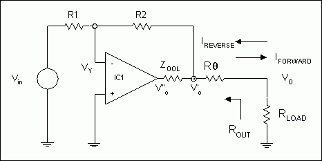
Figure 1. Simple passive matching
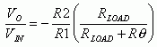
Note that in Figure 1, the load current IFORWARD is determined by VO / RLOAD.
When VIN is equal to zero, the composite output impedance ROUT is determined by VO / IREVERSE.
Here, the closed-loop output impedance of the default operational amplifier maintains a very low resistance value over a wide frequency band and can be ignored. Therefore, the output impedance is set by the selected resistor. In Figure 1, the series resistance RΘ sets the output equivalent impedance of IC1. RΘ = RLOAD = ROUT for correct backward matching. The operational amplifier open loop output impedance is expressed as ROOL.
The voltage gain is given by:
The error term is given by:
The output impedance is given by:
The error term is given by:
The error caused by the limited open-loop gain (AOP-AMP) of the operational amplifier is given.
Assume that the open-loop gain of an ideal operational amplifier is infinite.

Assume that the open-loop gain of an ideal operational amplifier is infinite.
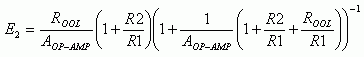
The advantages of Figure 1: Simple, choose RΘ to meet the required matching value. Appropriate short circuit protection. There is no first-order crosstalk between R1-R2 and RΘ. Support inverting and in-phase amplification. Disadvantages of Figure 1: When RΘ = RLOAD (backward matching), there is at least 6dB loss between the amplifier output pin (V'O) and the load drive point (VO). The maximum output peak-to-peak voltage swing is always less than half of the total power supply voltage. The gain bandwidth of the op amp is required to be doubled. The open-loop output impedance of the op amp affects high-frequency results. Fortunately, the output impedance active combination can find a way to set the output impedance and reduce the gain loss. Carefully use the positive feedback of the voltage differential amplifier to increase the output current detection resistor with a smaller resistance to achieve the desired final value.
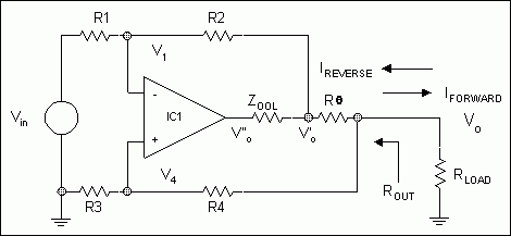
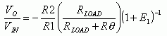
Figure 2. Active op amp matching
Note that in Figure 2, the load current IFORWARD is determined by VO / RLOAD.
When VIN is equal to zero, the combined output impedance ROUT is determined by VO / IREVERSE.
The single operational amplifier shown in Figure 2 has both positive and negative feedback loops, which set the gain and output impedance. RΘ is connected in series with the load to sample the load current. The positive feedback of R3 and R4 is used to amplify the equivalent value of RΘ. In order to keep the circuit stable, it is necessary to dominate negative feedback, which limits the gain.
Including the open-loop output impedance of the op amp, at the high-frequency end where the loop gain begins to decay, allows ROOL to approach RΘ.
The voltage gain shown in Figure 2 is given by:
The error term is given by:

Figure 2 The output impedance is given by:

The error due to the limited open-loop gain of the operational amplifier is given.
Note that the input and output signals of the circuit in Figure 2 are inverted.
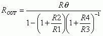
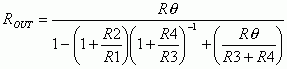
Assuming that the ideal operational amplifier open-loop gain is infinite, the output impedance is:
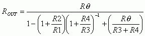
Generally speaking, the term [RΘ / [R3 + R4]] <<< [1 + R2 / R1] [1 + R4 / R3] -1, so it can be ignored.
Suppose the ideal operational amplifier open-loop gain is infinite, and the voltage gain is:
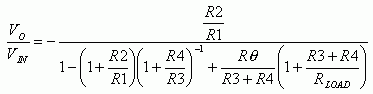
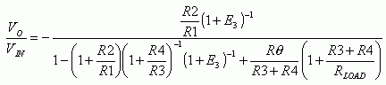
Bring the output impedance back into the gain formula:
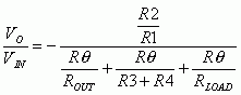
Generally, in reverse matching applications, RLOAD = ROUT. therefore:

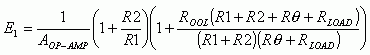
The advantages of Figure 2: greatly reduce the loss between the amplifier output (V'O) and the load drive point (VO). If RΘ = 0.1RLOAD, the loss is only 0.83dB. In other words, compared with the case of passive matching, the peak-to-peak output voltage swing of a given power supply is greatly improved. The main output has proper short circuit protection. Easy to use. Disadvantages of Figure 2: Positive feedback and negative feedback coexist. To maintain stability, it is necessary to always maintain negative feedback as the main factor. There is crosstalk between R1-R4, which is only suitable for the case of fixed gain and matching. Only applicable to inverting amplification architecture. Compared with a completely negative feedback architecture, positive feedback will increase distortion. There are several simple methods for measuring output impedance to measure the impedance mode of the circuit's equivalent output matching. The output impedance of the circuit under test is measured as shown in Figure 3, and the input of the circuit under test is grounded.
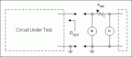
Figure 3. Output impedance measurement
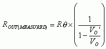
The simplest method in Figure 3a is to set RSET for a specific frequency so that | E2 | is equal to ½ | E1 |. The equivalent value of RSET is equal to the ZOUT of the circuit under test. At the test frequency, ZOUT appears as a pure resistance. Any reactive component introduces large errors in the so-called "6dB" method.
A more accurate method is to adjust RSET so that | E2 | is less than | E1 | 20dB, thus:
| ROUT | = RSET / 9
In particular, RSET can be fixed at 10 times the nominal resistance to be measured, and the ratio of E1 and E2 results in a "ZOUT" value.
If the ratio is 40dB:
| ROUT | is determined by RSET / 99.
Very careful when using the 40dB ratio, because the source voltage may be greater than the breakdown voltage of the circuit under test, depending on whether a low-voltage operational amplifier is used.
The second method is to use a suitable network analyzer.
The third method is the active impedance boosting technique, which directly measures the voltage and phase on the current-sense resistor RΘ. From the voltage difference, the combined output impedance can be derived as:
Please refer to Figure 2.
According to Figure 2, consider the effect of R3 and R4 in parallel with the output.

The input drive voltage from the test source is VO (in Figure 2), and the reflected voltage output from the operational amplifier is VO '(in Figure 2). A vector voltmeter can be used to extract the amplitude and phase difference. The VO '/ VO ratio is further modified by Cosq. The biggest disadvantage of this method is that when a relatively large signal level occurs, a small voltage difference on RΘ needs to be determined. If the design requires minimum loss between the amplifier and the final output under a specific output impedance, the circuit shown in Figure 2 can be selected. Both RLOAD and ROUT are known quantities. Choose RΘ as small as possible to ensure the stability of the entire circuit.
How much should RΘ "lift"? A reasonable upper limit is x10 (ie, RΘ = 0.1 RLOAD). This will produce a matching loss of 0.83dB. Each situation should be analyzed in detail, however, certain variables, such as open-loop output resistance, are difficult to be consistent with data specifications. The more the resistance is raised, the greater the positive feedback, the phase margin is reduced, and the closed-loop distortion is increased. The final choice of "boost" value will be the best compromise between matching loss and other closed-loop parameters, and an op amp with unity gain stability should be selected.
Make sure that the negative feedback loop time constant controls the entire loop, which means that ideally, the positive feedback loop should begin to decay before the negative feedback loop. Please refer to Figure 2, the first-order time constant (TC) of the negative feedback loop is:

The time constant of the positive feedback loop is:
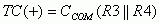
CCOM = the common-mode capacitance of the input of the non-inverting and inverting terminals of the op amp. Set: TC (-) <TC (+).
Assume that the input capacitance of the op amp is larger than the stray capacitance of the feedback loop resistance. In wideband applications, it is best to divide R1-R4 into two resistors of equal resistance to effectively reduce stray capacitance.
If the actual circuit is not self-excited, there may be in-band response spikes. A small signal (50mV to 100mV) sine wave scanning circuit can be used to check this, determine and draw a closed-loop frequency response (with load), and adjust the feedback time constant to correct any in-band spikes.
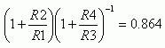
Example 1600Ω single-ended audio cable is actively matched.
Power supply voltage = + 5V
Gain = 1 (0dB)
ROUT = RLOAD = 600Ω
Select matching loss = 1dB
The MAX4475 op amp was chosen because it has extremely low distortion, and has excellent bandwidth, output drive capability, and unity gain stability.

ROUT = RLOAD, gain = 1.
For testing purposes, RLOAD = 600R and RΘ = 75R are preferred. RΘ = 0.125RLOAD.
R2 = 0.25R1
Let R1 = 10k, then R2 = 2.5k. Use R2 = 2.4k + 100R. Then:

Assuming RΘ, RLOAD = ROUT, as shown previously.
This ratio provides the RΘ boost value.
R4 = 0.428R3
Let R3 = 10k. Then, R4 = 4.28k. Use R4 = 4.3k.
Figure 4. Example 1 (for simplicity, power supply decoupling is not marked)
Table 1. Gain and frequency [0dB = 137.5mVRMS]
Table 2. RSET = 6.2kΩ (Figure 3) 0dB = 486mVRMS voltage difference
Calculated gain = -0.18dB, the value is shown above.
Calculate the output impedance = 572Ω. This value is obtained by subtracting the calculated value from R3 + R4 || ROUT.
Example 250Ω single-ended active matched broadband cable driver.
Power supply voltage = + 5V
Gain = 1 (0dB)
ROUT = RLOAD = 50Ω
Select matching loss = 1dB
The MAX4265 op amp was chosen because it has extremely low distortion, and has excellent bandwidth, output drive capability, and unity gain stability.
For 1dB matching loss.

For testing purposes, RLOAD = 50R and RΘ = 6.8R are preferred. RΘ = 0.136RLOAD.
R2 = 0.272R1
Let R1 = 1k. Then, R2 = 272R. Use R2 = 270R as the first choice. Then:
When RΘ and RLOAD = ROUT, as shown above.
This ratio provides an increase in RΘ.
R4 = 0.472R3
Let R3 = 1k. Then, R3 = 472R. Use R3 = 470R as the first choice.
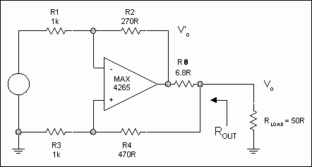
Figure 5. Example 2 (for simplicity, power supply decoupling is not marked)
Table 3. Gain and frequency 0dB = 70mVRMS
Table 4. RSET = 510R (Figure 3) 0dB = 225mVRMS voltage difference
Calculated gain = -0.63dB, the value is shown above, considering the additional 50Ω source impedance not included in R1
Calculate the output impedance = 45.5Ω. This value is obtained by subtracting the calculated value from R3 + R4 || ROUT. Conclusion In the commonly used voltage mode differential operational amplifiers, careful use of positive feedback can result in a greater output impedance than negative feedback. Suitable for the design of single-supply amplifiers, the driver stage amplifier must drive the source impedance load. Compared with standard passive matching, a matching "gain" of 5dB can be obtained.
Matching requirements In transmission line drive applications, the circuit output impedance is very important. The transmission line impedance is determined by the physical dimensions of the conductor and the insulator. It must be matched at the sending end and the receiving end at the same time to minimize signal reflection. When the characteristic impedances of the driving circuit and the receiving end are not completely matched, all the signal energy cannot be transmitted to the load. Part of the energy is reflected back, distorting the signal transmitted to the load (sometimes even canceling it completely).
RF engineers need accurate 50Ω matching on coaxial cables, video transmission engineers need accurate 75Ω matching on the cables used, and broadcast equipment engineers need accurate 600Ω matching on audio circuits. Other standard matching values ​​are 110Ω, 120Ω and 500Ω. The matching requirements are not limited to analog signals. Digital signals also rely on precise line matching to achieve error-free high-speed transmission. The common method of passive impedance matching and matching is to use a buffer amplifier with a lower output impedance and add a series resistance that meets the requirements. This method is relatively simple when the pre-buffer amplifier has a low output impedance over the entire bandwidth.
An important drawback of the simple method of adding resistors is that there is a 6dB signal loss between the buffered output and the matched load, resulting in a serious loss of signal margin, especially in a single-supply power supply system.
In the closed-loop buffer amplifier shown in Figure 1, a series resistor is added outside the feedback loop to set the equivalent output impedance of the amplifier.
Figure 1. Simple passive matching
Note that in Figure 1, the load current IFORWARD is determined by VO / RLOAD.
When VIN is equal to zero, the composite output impedance ROUT is determined by VO / IREVERSE.
Here, the closed-loop output impedance of the default operational amplifier maintains a very low resistance value over a wide frequency band and can be ignored. Therefore, the output impedance is set by the selected resistor. In Figure 1, the series resistance RΘ sets the output equivalent impedance of IC1. RΘ = RLOAD = ROUT for correct backward matching. The operational amplifier open loop output impedance is expressed as ROOL.
The voltage gain is given by:
The error term is given by:
The output impedance is given by:
The error term is given by:
The error caused by the limited open-loop gain (AOP-AMP) of the operational amplifier is given.
Assume that the open-loop gain of an ideal operational amplifier is infinite.
Assume that the open-loop gain of an ideal operational amplifier is infinite.
The advantages of Figure 1: Simple, choose RΘ to meet the required matching value. Appropriate short circuit protection. There is no first-order crosstalk between R1-R2 and RΘ. Support inverting and in-phase amplification. Disadvantages of Figure 1: When RΘ = RLOAD (backward matching), there is at least 6dB loss between the amplifier output pin (V'O) and the load drive point (VO). The maximum output peak-to-peak voltage swing is always less than half of the total power supply voltage. The gain bandwidth of the op amp is required to be doubled. The open-loop output impedance of the op amp affects high-frequency results. Fortunately, the output impedance active combination can find a way to set the output impedance and reduce the gain loss. Carefully use the positive feedback of the voltage differential amplifier to increase the output current detection resistor with a smaller resistance to achieve the desired final value.
Figure 2. Active op amp matching
Note that in Figure 2, the load current IFORWARD is determined by VO / RLOAD.
When VIN is equal to zero, the combined output impedance ROUT is determined by VO / IREVERSE.
The single operational amplifier shown in Figure 2 has both positive and negative feedback loops, which set the gain and output impedance. RΘ is connected in series with the load to sample the load current. The positive feedback of R3 and R4 is used to amplify the equivalent value of RΘ. In order to keep the circuit stable, it is necessary to dominate negative feedback, which limits the gain.
Including the open-loop output impedance of the op amp, at the high-frequency end where the loop gain begins to decay, allows ROOL to approach RΘ.
The voltage gain shown in Figure 2 is given by:
The error term is given by:
Figure 2 The output impedance is given by:
The error due to the limited open-loop gain of the operational amplifier is given.
Note that the input and output signals of the circuit in Figure 2 are inverted.
Assuming that the ideal operational amplifier open-loop gain is infinite, the output impedance is:
Generally speaking, the term [RΘ / [R3 + R4]] <<< [1 + R2 / R1] [1 + R4 / R3] -1, so it can be ignored.
Suppose the ideal operational amplifier open-loop gain is infinite, and the voltage gain is:
Bring the output impedance back into the gain formula:
Generally, in reverse matching applications, RLOAD = ROUT. therefore:
The advantages of Figure 2: greatly reduce the loss between the amplifier output (V'O) and the load drive point (VO). If RΘ = 0.1RLOAD, the loss is only 0.83dB. In other words, compared with the case of passive matching, the peak-to-peak output voltage swing of a given power supply is greatly improved. The main output has proper short circuit protection. Easy to use. Disadvantages of Figure 2: Positive feedback and negative feedback coexist. To maintain stability, it is necessary to always maintain negative feedback as the main factor. There is crosstalk between R1-R4, which is only suitable for the case of fixed gain and matching. Only applicable to inverting amplification architecture. Compared with a completely negative feedback architecture, positive feedback will increase distortion. There are several simple methods for measuring output impedance to measure the impedance mode of the circuit's equivalent output matching. The output impedance of the circuit under test is measured as shown in Figure 3, and the input of the circuit under test is grounded.
Figure 3. Output impedance measurement
The simplest method in Figure 3a is to set RSET for a specific frequency so that | E2 | is equal to ½ | E1 |. The equivalent value of RSET is equal to the ZOUT of the circuit under test. At the test frequency, ZOUT appears as a pure resistance. Any reactive component introduces large errors in the so-called "6dB" method.
A more accurate method is to adjust RSET so that | E2 | is less than | E1 | 20dB, thus:
| ROUT | = RSET / 9
In particular, RSET can be fixed at 10 times the nominal resistance to be measured, and the ratio of E1 and E2 results in a "ZOUT" value.
If the ratio is 40dB:
| ROUT | is determined by RSET / 99.
Very careful when using the 40dB ratio, because the source voltage may be greater than the breakdown voltage of the circuit under test, depending on whether a low-voltage operational amplifier is used.
The second method is to use a suitable network analyzer.
The third method is the active impedance boosting technique, which directly measures the voltage and phase on the current-sense resistor RΘ. From the voltage difference, the combined output impedance can be derived as:
Please refer to Figure 2.
According to Figure 2, consider the effect of R3 and R4 in parallel with the output.
The input drive voltage from the test source is VO (in Figure 2), and the reflected voltage output from the operational amplifier is VO '(in Figure 2). A vector voltmeter can be used to extract the amplitude and phase difference. The VO '/ VO ratio is further modified by Cosq. The biggest disadvantage of this method is that when a relatively large signal level occurs, a small voltage difference on RΘ needs to be determined. If the design requires minimum loss between the amplifier and the final output under a specific output impedance, the circuit shown in Figure 2 can be selected. Both RLOAD and ROUT are known quantities. Choose RΘ as small as possible to ensure the stability of the entire circuit.
How much should RΘ "lift"? A reasonable upper limit is x10 (ie, RΘ = 0.1 RLOAD). This will produce a matching loss of 0.83dB. Each situation should be analyzed in detail, however, certain variables, such as open-loop output resistance, are difficult to be consistent with data specifications. The more the resistance is raised, the greater the positive feedback, the phase margin is reduced, and the closed-loop distortion is increased. The final choice of "boost" value will be the best compromise between matching loss and other closed-loop parameters, and an op amp with unity gain stability should be selected.
Make sure that the negative feedback loop time constant controls the entire loop, which means that ideally, the positive feedback loop should begin to decay before the negative feedback loop. Please refer to Figure 2, the first-order time constant (TC) of the negative feedback loop is:
The time constant of the positive feedback loop is:
CCOM = the common-mode capacitance of the input of the non-inverting and inverting terminals of the op amp. Set: TC (-) <TC (+).
Assume that the input capacitance of the op amp is larger than the stray capacitance of the feedback loop resistance. In wideband applications, it is best to divide R1-R4 into two resistors of equal resistance to effectively reduce stray capacitance.
If the actual circuit is not self-excited, there may be in-band response spikes. A small signal (50mV to 100mV) sine wave scanning circuit can be used to check this, determine and draw a closed-loop frequency response (with load), and adjust the feedback time constant to correct any in-band spikes.
Example 1600Ω single-ended audio cable is actively matched.
Power supply voltage = + 5V
Gain = 1 (0dB)
ROUT = RLOAD = 600Ω
Select matching loss = 1dB
The MAX4475 op amp was chosen because it has extremely low distortion, and has excellent bandwidth, output drive capability, and unity gain stability.
ROUT = RLOAD, gain = 1.
For testing purposes, RLOAD = 600R and RΘ = 75R are preferred. RΘ = 0.125RLOAD.
R2 = 0.25R1
Let R1 = 10k, then R2 = 2.5k. Use R2 = 2.4k + 100R. Then:
Assuming RΘ, RLOAD = ROUT, as shown previously.
This ratio provides the RΘ boost value.
R4 = 0.428R3
Let R3 = 10k. Then, R4 = 4.28k. Use R4 = 4.3k.
Figure 4. Example 1 (for simplicity, power supply decoupling is not marked)
Table 1. Gain and frequency [0dB = 137.5mVRMS]
| Frequency (kHz) | Gain (dB) | Phase (Deg) |
| 100 | -0.3 | 5.6 |
| 220 | -0.5 | 14 |
| 430 | -1.0 | twenty three |
| 580 | -1.5 | 29 |
| 710 | -2.0 | 33 |
| 830 | -2.5 | 37 |
| 940 | -3.0 | 39 |
| 1050 | -3.5 | 47 |
| 1170 | -4.0 | 52 |
| 1370 | -5.0 | 62 |
Table 2. RSET = 6.2kΩ (Figure 3) 0dB = 486mVRMS voltage difference
| Frequency (kHz) | dB (across 6.2kΩ) | ROUT (Ω) |
| 100 | -21.5 | 517 |
| 220 | -21.8 | 502 |
| 430 | -22.4 | 468 |
| 580 | -23.2 | 429 |
| 710 | -twenty four | 392 |
| 830 | -24.6 | 364 |
| 940 | -25.2 | 340 |
| 1050 | -26 | 313 |
| 1170 | -26.6 | 287 |
| 1370 | -28 | 249 |
Calculated gain = -0.18dB, the value is shown above.
Calculate the output impedance = 572Ω. This value is obtained by subtracting the calculated value from R3 + R4 || ROUT.
Example 250Ω single-ended active matched broadband cable driver.
Power supply voltage = + 5V
Gain = 1 (0dB)
ROUT = RLOAD = 50Ω
Select matching loss = 1dB
The MAX4265 op amp was chosen because it has extremely low distortion, and has excellent bandwidth, output drive capability, and unity gain stability.
For 1dB matching loss.
For testing purposes, RLOAD = 50R and RΘ = 6.8R are preferred. RΘ = 0.136RLOAD.
R2 = 0.272R1
Let R1 = 1k. Then, R2 = 272R. Use R2 = 270R as the first choice. Then:
When RΘ and RLOAD = ROUT, as shown above.
This ratio provides an increase in RΘ.
R4 = 0.472R3
Let R3 = 1k. Then, R3 = 472R. Use R3 = 470R as the first choice.
Figure 5. Example 2 (for simplicity, power supply decoupling is not marked)
Table 3. Gain and frequency 0dB = 70mVRMS
| Frequency (MHz) | Gain (dB) | Phase (Deg) |
| 1.0 | -0.3 | 0 |
| 2.0 | -0.3 | -3.5 |
| 4.0 | -0.4 | -10.25 |
| 6.0 | -0.7 | -16.5 |
| 8.0 | -1.0 | -23.5 |
| 10.0 | -1.3 | -30 |
| 15.0 | -2.3 | -44 |
| 20.0 | -3.5 | -58 |
| 30.0 | -7.0 | 87 |
Table 4. RSET = 510R (Figure 3) 0dB = 225mVRMS voltage difference
| Frequency (MHz) | dB Across 510Ω | Phase (Deg) | ROUT (Ω) |
| 1.0 | -twenty one | -3.2 | 45.4 |
| 2.0 | -twenty one | -4.4 | 45.4 |
| 4.0 | -twenty one | -7.25 | 45.4 |
| 8.0 | -21.8 | -14.5 | 41.45 |
| 10 | -22.1 | -15.5 | 40 |
| 20 | -23.7 | -twenty one | 33.3 |
Calculated gain = -0.63dB, the value is shown above, considering the additional 50Ω source impedance not included in R1
Calculate the output impedance = 45.5Ω. This value is obtained by subtracting the calculated value from R3 + R4 || ROUT. Conclusion In the commonly used voltage mode differential operational amplifiers, careful use of positive feedback can result in a greater output impedance than negative feedback. Suitable for the design of single-supply amplifiers, the driver stage amplifier must drive the source impedance load. Compared with standard passive matching, a matching "gain" of 5dB can be obtained.
Led Ceiling Fan,Two Blades Ceiling Fan,Two Blades Energy Saving Fan,Two Blades Electric Ceiling Fan
Jiangmen MagicPower Electrical Appliances Co.,Ltd. , https://www.magicpowerfan.com