IntroducTIon to DS1868The DS1868 is a dual digital potenTIometer with a 3-wire interface. This application note will describe how to interface a Dallas Semiconductor 3-wire device to a microcontroller with a SPITM interface.
Comparing SPI And 3-Wire InterfacesThe SPI and 3-wire are different serial interfaces but they are compatible. The following section describes the differences.
Serial Peripheral Interface (SPI) The SPI has 4 signals: SDO, SDI, SCK, and active-low SS. The SDO signal is data out, SDI is data in, SCK is the clock, and active-low SS is the slave select .
3-Wire Serial InterfaceThe 3-wire serial interface has 4 signals: DQ, Cout, active-low RST and CLK. The data in is on the DQ signal, data out is on the Cout signal, active-low RST signal enables the 3 -wire interface, and CLK is the clock.
Table 1. 3-Wire vs. SPI Interface.
| Serial Interface | Signal names | Signal Descriptions | BUS Speed ​​(Typical) | Data Format |
| 3-WIRE | DQ | Data In | 500kHz to 5 MHz | LSB first, MSB last |
| Cout | Data Out | |||
| active-low RST | active-low Reset | |||
| CLK | Clock | |||
| SPI | SDI | Data In | 10MHz | MSB first, LSB last |
| SDO | Data Out | |||
| active-low SS | active-low Slave Select | |||
| SCK | Clock |
Note: In this application note, active-low SS is not used (only used when in slave mode).
Writing / Reading Bytes Writing Data to DS1868The microcontroller, which contains an SPI interface, transmits and receives data in multiples of 8 bits. Therefore, 7 additional bits need to be sent along with the 17 bits of data for a total of 3 bytes. The microcontroller sends the MSB first. When the microcontroller writes data to the DS1868, the first 7 bits of the first byte are pushed out of the shift register and b0 contains the LSB of the first byte (see Figure 1).
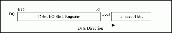
Figure 1. Shift register with 7 additional bits during a write. Reading Data from the DS1868 When the microcontroller reads the data from the DS1868, the stack select bit (b0) gets transmitted first, then the MSB of Pot 1 (b1) and so on (see Figure 2). When reading, the extra 7 bits are located in the third byte.
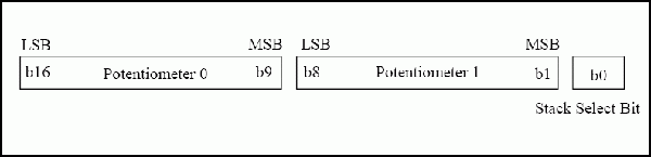
Figure 2. 17-Bit Shift register.
The following is an example of how bytes are written and read. In this example the stack select bit selects Pot 1. Pot 1 is programmed to 0Fh and Pot 0 is programmed to 55h. The value of the selected pot's wiper will be on the SOUT pin. The three bytes that are written to the DS1868 are 01h, 0Fh, and 55h. The leading zeros of 01h are the 7 additional bits. The microcontroller sends the MSB first so the leading 7 zeros are first transmitted. These leading zeros fall off the end and the '1' ends up in b0. Pot 1 will have the first 4 bits filled with 0s and the last 4 bits filled with 1s. The MSB in Pot 0 will be a '0' with the remaining bits alternating between 1 and 0.
Byte 0: 00000001b (01h) The additional bits are underlined.
Byte 1: 00001111b (0Fh)
Byte 2: 01010101b (55h)
When the data is read, b0 is the first bit out. The 3 bytes that are output will now read as follows:
Byte 0: 10000111 (87h)
Byte 1: 10101010 (AAh)
Byte 2: 10000000 (80h) The additional bits are underlined.
The 7 additional bits are now at the end of Byte 2.
More examples of converting written to read data are in Table 2.
The software compares the bytes written to the bytes read from the DS1868 (see the Appendix).
Table 2. Converting Data Bytes Between Writing and Reading
| 3 Bytes Written (hex) | 3 Bytes Written (binary) | Pot Settings SS Pot1 Pot0 | 3 Bytes Read (hex) | 3 Bytes Read (binary) |
| 01h FFh 80h | 00000001 11111111 10000000 | 1 FFh 80h | FFh C0h 00h | 11111111 11000000 00000000 |
| 01h 80h 80h | 00000001 10000000 10000000 | 1 FFh 80h | C0h 40h 00h | 11000000 01000000 00000000 |
| 00h 80h 0Fh | 00000000 10000000 00001111 | 0 80h 0Fh | 40h 07h 80h | 01000000 00000111 10000000 |
Hardware ConfigurationA schematic of the board is shown in Figure 3.
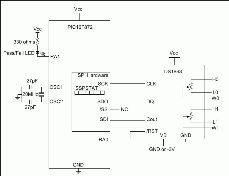
Figure 3. Board Schematic. Software Configuration The software configuration is for a PIC16F872.
Port SettingsThe TRISx register sets the pins to an input (1) or an output (0). The PORTA register will drive active-low RST and LED to 5V or 0V.
TRISA = --1xxx00—RA5active-low SS is set to an input. This is used to enable the serial port. RA0 and RA1 are set to outputs for the active-low RST and LED
TRISB = Not used
TRISC = xx010xxx—Clears SCK and SDO, sets SDI
The active-low RST pin needs to be set before data is transmitted / received and then needs to be cleared after the transaction is complete.
SPI SettingsSSPSTAT = 01000000 (40h) —bit SMP = 0, bit CKE = 1
When SMP = 0, the input data is sampled at the end of data output time.
When CKE = 1, transmit happens on transition from active clock state to idle clock state when CKP = 0.
The SSPSTAT register sets up the clock and data to have the correct timing to interface with the DS1868.
SSPCON = 00100001 (21h) —bit SSPEN = 1, bit SSPM3-0 = 0001
SSPEN = 1 enables the serial port.
SSPM3-0 selected the clock frequency. SSPM3-0 = 0001 = Fosc / 16 = 20MHz / 16 = 1.25MHz
The DS1868 has a maximum clock rate of 10MHz.
CodeThe Appendix contains the assembly code to write, read, and compare potentiometer data.
Each port that is used needs to be initialized in addition to the SPI port. The potentiometers also need to be initialized to zero. Then data can be written to the potentiometers.
SPI TimingUsing the register settings described above, the microcontroller produces the following timing signals.
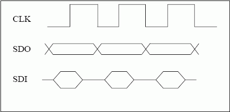
Figure 4. SPI timing diagram.
Transmission of the data on SDO is completed on the falling edge of the clock. Data is received on SDI during the clock cycle. The following are diagrams of the potentiometer data being received and transmitted. Figure 5 shows 01h, FFh, and 80h being sent to the DS1868 on the SDO line. SDI contains the data the DS1868 sends back to the microcontroller. The data on SDI is FFh, C0h, and 00h. See Table 2 for more information on converting data.
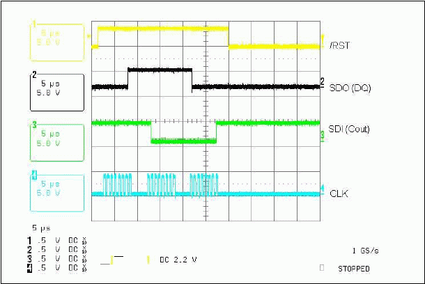
Figure 5. Data transmitted / received.
Transmission of the data on SDO is completed on the falling edge of the clock. Data is received on SDI during the clock cycle. The following are diagrams of the potentiometer data being received and transmitted. Figure 5 shows 01h, FFh, and 80h being sent to the DS1868 on the SDO line. SDI contains the data the DS1868 sends back to the microcontroller. The data on SDI is FFh, C0h, and 00h. See Table 2 for more information on converting data.
Figure 6 shows 01h, 80h, and 80h being sent to the DS1868. The data is then compared to C0h, 40h, and 00h. See Table 2 for more information on converting data.
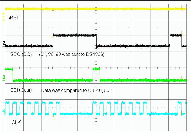
Figure 6. Data transmitted / received (detail). Appendix Assembly Code using the PIC16F872; *****************; App Note Code; The following code was developed on the PIC16F872 .; ***************** LIST p = 16F872 #INCLUDE GOTO MAIN; *** Subroutines ***; Delay for LED WAIT MOVWF 0x23 MOVLW 0x20 MOVWF 0x20 DEC1 DECFSZ 0x20 GOTO LOOP1 RETURN LOOP1 MOVLW 0xFF MOVWF 0X21 DEC2 DECFSZ 0X21 GOTO LOOP2 GOTO DEC1 LOOP2 MOVLW 0xFF MOVWF 0x22 DEC3 DECFSZ 0X22 GOTO DEC3 GOTO DEC2; ************************* ************; Test to Determine is TX is Complete DONE BSF STATUS, RP0; Select Bank 1 BTFSS SSPSTAT, 0; Test SSPBUF to determine if TX is complete GOTO DONE RETURN; **** **********************************; Initialize PORTA INITA BCF STATUS, RP0; Select Bank 0 BCF STATUS, RP1 CLRF PORTA; Clear output data latches BSF STATUS, RP0; Select Bank 1 MOVLW 0x06; All outputs set digital MOVWF ADCON1 MOVLW 0x20; Value used to initialize data direction MOVWF TRISA; LED and active-low RST outputs BCF STATUS, RP0; Select Bank 0 BCF STATUS, RP1 BSF PORTA, 1; LED off BCF PORTA, 0; active-low RST = 0V RETURN; ******************* *******************; Initialize PORTC INITC BCF STATUS, RP0; Select Bank 0 BCF STATUS, RP1 CLRF PORTC; Clear output data latches BSF STATUS, RP0; Select Bank 1 MOVLW 0x10; Value used to initialize data direction MOVWF TRISC; Clears SCK and SDO, sets SDI RETURN; ***************************** *********; Initialize SPI SPI BSF STATUS, RP0; Select Bank 1 MOVLW 0x40 MOVWF SSPSTAT; SMP = 0, CKE = 1: These bits set up the data & clock. BCF STATUS, RP0; Select Bank 0 BCF STATUS, RP1 MOVLW 0x21 MOVWF SSPCON; SSPEN = 1, CKP = SSPMx = 0001 (Fosc / 16) RETURN; ************************ ***************; Initialize POT1 WRITE0 BCF STATUS, RP0; Select Bank 0 BCF STATUS, RP1 BSF PORTA, 0; active-low RST = 5V MOVLW 0x00; Clear Byte 0 MOVWF SSPBUF CALL DONE; Test SSPBUF to determine if TX is complete BCF STATUS, RP0; Select Bank 0 BCF STATUS, RP1 MOVLW 0x00; Clear Byte 1 MOVWF SSPBUF CALL DONE; Test SSPBUF to determine if TX is complete BCF STATUS, RP0; Select Bank 0 BCF STATUS, RP1 MOVLW 0x00; Clear Byte 2 MOVWF SSPBUF CALL DONE; Test SSPBUF to determine if TX is complete BCF STATUS, RP0; Select Bank 0 BCF STATUS, RP1 BCF PORTA, 0; active-low RST = 0V RETURN; ****************************** *********; Write to Pot1 WRITE BCF STATUS, RP0; Select Bank 0 BCF STATUS, RP1 BSF PORTA, 0; active-low RST = 5V MOVLW 0x01; Stack Select bit = 1 (Byte 0) MOVWF SSPBUF CALL DONE BCF STATUS, RP0; Select Bank 0 BCF STATUS, RP1 MOVLW 0xFF; Pot1 = FF (Byte 1) MOVWF SSPBUF CALL DONE BCF STATUS, RP0; Select Bank 0 BCF STATUS, RP1 MOVLW 0x80; Pot0 = 80 (Byte 2 ) MOVWF SSPBUF CALL DONE BCF STATUS, RP0; Bank0 BCF STATUS, RP1 BCF PORTA, 0; active-low RST = 0V RETURN; ********************** *****************; Compare Data Transmitted and Received CMPR BCF STATUS, RP; Select Bank 0 BCF STATUS, RP1 BSF PORTA, 0; active-low RST = 5V MOVLW 0x01; Write Byte 0 MO VWF SSPBUF BCF PORTA, 1; LED on CALL DONE BCF STATUS, RP0; Select Bank 0 BCF STATUS, RP1 MOVF SSPBUF, 0; Read Byte 0 XORLW 0xFF BTFSS STATUS, 2 GOTO FAIL MOVLW 0xFF; Write Byte 1 MOVWF SSPBUF CALL DONE BCF STATUS, RP0; Select Bank 0 BCF STATUS, RP1 MOVF SSPBUF, 0; Read Byte 1 XORLW 0xC0 BTFSS STATUS, 2 GOTO FAIL MOVLW 0x80; Write Byte 2 MOVWF SSPBUF CALL DONE BCF STATUS, RP0; Select Bank 0 BCF STATUS, RP1V SSPBUF, 0; Read Byte 2 ANDLW 0x80 BTFSS STATUS, 2 GOTO FAIL BCF PORTA, 0; active-low RST = 0V GOTO PASS RETURN; ******************** *******************; If Compare Fails FAIL BCF STATUS, RP0; Select Bank 0 BCF STATUS, RP1 CLRF PORTA; Initialize PORTA by clearing output data latches BSF STATUS, RP0 ; Select Bank 1 MOVLW 0x06; All outputs set digital MOVWF ADCON1 MOVLW 0x20; Value used to initialize data direction MOVWF TRISA; LED on and active-low RST high BCF STATUS, RP0; Select Bank 0 BCF STATUS, RP1 BCF PORTA, 1; LED on CALL WAIT BSF PORTA, 1; LED off CALL W AIT GOTO FAIL; Repeat blinking LED; ***********************************; If Compare Passes PASS BCF STATUS , RP0; Select Bank 0 BCF STATUS, RP1 BCF PORTA, 1; LED on GOTO PASS; LED remains on; ****** THE MAIN PROGRAM ******** MAIN CALL INITA; Initialize PORTA CALL INITC; Initialize PORTC CALL SPI; Initialize SPI CALL WRITE0; Initialize Pots CALL WRITE; Write data to pots CALL CMPR Compare data written to pots w / data received from pots END
High-mast lights are quite different in nature from more typical street or roadway lights. High-mast fixtures are regularly mounted at 60 ft to more than 100 ft above ground level and occasionally as high as 250 ft. Normal Street Lights are typically mounted at heights lower than 60 ft, and many are in the 30-ft range.
The applications for high-mast lights include installations at transportation terminals, other large, outdoor maintenance or storage yards, and specialty roadway applications. The aforementioned freeway interchange installations are probably the most common roadway application, although you will find some high-mast lights within municipalities in busy areas
Highway High Mast Light,Galvanized Highway High Mast Light,Highway High Mast Lighting Pole,Highway Lighting Pole
Shenzhen Ri Yue Guang Hua Technology Co., Ltd. , https://www.ledlightinside.com