IntroductionEmerging wireless communications standards (wide-band, multi-carrier) demand increasingly lower distortion and noise specifications.The digital-to-analog converters (DACs) in the transmitter (Tx) circuits are the key components for analog signal generation. They can significantly influence the system's ultimate dynamic performance.
The transmitter sections of multi-carrier base station transceiver systems for GSM / EDGE present a chanllenge to communication DAC manufacturers. Manufacturers need to supply higher resolution and faster update rates, at higher output frequencies, all while reducing noise and spurious emissions over a wide bandwidth .
As a result of these requirements, GSM / EDGE system designers consider communications DACs attractive only if they can meet key specifications in four major noise and distortion categories. These are: Spurious-free Dynamic Range (SFDR), Signal-to-Noise Ratio ( SNR), Intermodulation Distortion (IMD), and Multi-tone power ratio (MTPR). All four parameters are critical in ensuring that the Tx system meets required spurious and IMD targets. DAC Dynamic Performance Requirements for GSM / EDGETo specify noise and spurious emissions from base stations, a so-called GSM / EDGE Tx mask is used to identify the DAC requirements for these parameters. This mask shows that the allowable levels for noise and spurious emissions are dependent on the offset frequency from the transmitted carrier frequency. The GSM / EDGE mask and its specifications are based on a single active carrier with any other carriers in the transmitter being disabled. Specifications displayed in Figure 1 support per-carrier output power levels of 20W or greater. Lower output power levels will yield less stringent emission requirements.
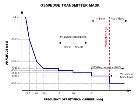
Figure 1. The Tx mask helps to identify the noise and distortion limits for DACs, used in the transmission path of a GSM / EDGE-based Base Station Transceiver System.
Spurious-free Dynamic Range (SFDR) GSM / EDGE systems require the analog signal synthesis circuit block (the DAC) to have spurious emission levels of less than -80dBc for offset frequencies ≥ 6MHz. Spurious products from the DAC can combine with both random noise and spurious products from other circuit elements. The spurious products from the DAC should therefore be backed off a further 6dB (minimum) to allow for these other sources.
The number of carriers and their signal levels with respect to the full-scale of the DAC also play an important role. Unlike a full-scale sine wave, the inherent nature of a multi-tone signal, in which the spectral energy of the signal is spread over a defined bandwidth, contains higher peak-to-rms ratios, raising the prospect for potential clipping, if the signal level hasn't been backed off appropriately. If a transmitter operates with four in-band carriers, each individual carrier must be operated at> 12dB below full-scale while eight carriers require an amplitude of> 18dB below full-scale to preclude waveform clipping.
Example: An EDGE-based modulation has a peak-to-rms ratio of 4dB for the 8-PSK (Phase-Shift Keying) modulation employed. This requires the carrier amplitude to be backed-off by another 4dB. An additional margin of- 6dB is used to compensate for other circuit elements. For systems with four / eight carriers per designated bandwidth, each individual carrier must satisfy an amplitude specification of -18dBFS / -24dBFS or less.
Signal-to-Noise Ratio (SNR) The SNR requirements for a GSM / EDGE-based system can again be derived from the GSM / EDGE Tx mask (Figure 1). With a worst-case noise level of -80dBc at frequency offsets of ≥ 6MHz and an assumed measurement bandwidth of 100kHz, the minimum noise density per Hertz is calculated as follows: SNRMIN = -80dB-10 × log10 (100 × 10³Hz)
SNRMIN = -130dB / Hz> Since random DAC noise will add to both the spurious tones and to random noise from other circuit elements, it is recommended to reduce the specification limits by about 10dB to allow for these additional noise contributions while maintaining compliance with the GSM / EDGE mask values.
| Number of Carriers | Carrier Amplitude | DAC SNR Requirement |
| 2 | -12dBFS | -152dBFS / Hz |
| 4 | -18dBFS | -158dBFS / Hz |
| 8 | -24dBFS | -160dBFS / Hz |
Intermodulation Distortion (IMD), and Multi-tone power ratio (MTPR) Other key factors in selecting a DAC for the Tx path of a multi-carrier GSM / EDGE system is the converter's ability to offer superior IMD and MTPR performance. Multiple carriers in a designated band will generate unwanted intermodulation distortion between the individual carrier frequencies. A multi-tone test vector usually consists of several equally spaced carriers, usually four, with identical amplitudes. Each of these carriers is representative of a channel within the defined bandwidth of interest . To verify MTPR, one or more tones are removed such that the intermodulation distortion performance of the DAC can be evaluated. Nonlinearities associated with the DAC will create spurious tones of which some may fall back into the area of ​​the removed tone, limiting a channel's carrier-to-noise ratio. Other spurious components falling outside the band of interest also may be important, depending on the system's spectral mas k and filtering requirements. Going back to the GSM / EDGE Tx mask, the IMD specification for adjacent carriers varies somewhat among the different GSM standards. For the PCS1800 and GSM850 standards, the DAC must meet an average IMD of -70dBc.
The following table summarizes the dynamic performance requirements for the entire Tx signal chain in a four-carrier GSM / EDGE-based system and compares the previously established converter requirements with a new generation high-dynamic performance DAC.
| Specification | Tx Output Level | DAC Requirements with Margins | MAX5195 Specifications |
| SFDR | 80dBc to 83dBc | 88dBc | 83dBc¹ |
| SNR | -133dBc / Hz | -158dBFS / Hz | -160dBFS / Hz |
| IMD | -70dBc | -75dBc | -77dBc |
| Carrier Amplitude | N / S | -18dBFS | -18dBFS |
The 14-bit, 260Msps MAX5195 is the first DAC, which is fully compatible with 4-carrier GSM / EDGE signal generation. It provides excellent dynamic performance and meets all of the GSM / EDGE spectral mask requirements.
The four-tone MTPR plot (Figure 2) demonstrates the DACs superior dynamic performance. The center frequency (fCENTER = 48.9583MHz) has been removed to allow detection and analysis of intermodulation or spurious components falling back into this empty spot from adjacent channels. The four carriers are observed over a 25MHz bandwidth and are equally spaced at 1MHz. The output amplitude has been backed-off by -18dBFS according to the GSM / EDGE spectral mask. Under these conditions, the DAC yields an IMD of -77dBc and an MTPR of -78dBc.
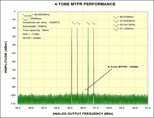
Figure 2. This spectrum plot depicts the four-tone MTPR performance at fCENTER = 48.9583MHz and fCLK = 260MHz of the MAX5195, which meets the most critical GSM / EDGE specifications. ConclusionFrom a system point of view, the ability of the DAC to keep high degrees of dynamic performance under multi-tone conditions, eases the transmitter path design. Traditionally, BTS systems would employ one converter per transmit channel. Now however a DAC with sufficiently high multi-tone performance, will help to simplify the transmitter architecture and reduces board space and cost by cutting down on the number of DACs required in such a system.
Notes1 Single-carrier SFDR observed within a 25MHz window. Although the DAC doesn't meet the SFDR specification completely, a lower single-tone SFDR can be accommodated and compensated for by frequency planning.
A similar version of this article appeared in the October 2002 issue of Electronic Products magazine.
HDI Printed Circuit Boards - High Density Interconnect PCB Technology
With the development of society, the progress of technology comes from people's constant pursuit of life and their yearning for higher quality of life. Personal consumer electronic products such as notebook computers, personal computers and mobile phones require lighter weight and smaller volume, while smaller volume requires smaller design accuracy and higher density. At the same time, the quality and speed of interconnection technology should be better. This requires designers who make these products to design better components to improve electrical performance, such as circuit boards and so on.
In order to manufacture PCB products of this kind, PCB manufacturers need more advanced manufacturing technology. Of course, from the point of view of product cost, it needs lower cost. This seems contradictory, but HDI PCB can solve this problem very well. HDI PCB has numerous advantages, such as high speed, small size and high frequency.
HDI PCB is the better option for high-layer count and costly laminated boards.
What is a HDI PCB, The definition of HDI PCB
HDI stands for High Density Interconnector, HDI Printed Circuit Board. A circuit board which has a higher wiring density per unit area as opposed to conventional board is called as HDI PCB. HDI PCBs have finer spaces and lines, minor vias and capture pads and higher connection pad density. It is helpful in enhancing electrical performance and reduction in weight and size of the equipment.
High density interconnect (HDI) PCBs represent one of the fastest-growing segments of the Printed Circuit Board market. Because of its higher circuitry density, the HDI PCB design can incorporate finer lines and spaces, smaller vias and capture pads, and higher connection pad densities. A high-density PCB features blind and buried vias and often contains microvias that are .006 in diameter or even less.
Regarding the electrical needs of high-speed signal, the board should have various features i.e. high-frequency transmission capability, impedance control, decreases redundant radiation, etc. The board should be enhanced in the density because of the miniaturization and arrays of the electronic parts. In addition, to the result of the assembling techniques of leadless, fine pitch package and direct chip bonding, the board is even featured with exceptional high-density.
There were a lot of different names for the PCB with such structures. For example, it was called SBU (Sequence Build up the Process) in European and American industry as the program production is in the constructive mode of sequence. It was called MVP (Microvia Process) in Japanese industry because the hole of such products is much smaller than the previous one. It was also called BUM (Build up Multilayer PCB Board ) because the traditional multilayer is known as MLB (Multilayer PCB Board).In order to avoid confusion, IPC Printed Circuit Association proposed to call it HDI (High Density Interconnection Technology) as the common name, but it can not reflect the characteristics of the circuit board. So the majority in the PCB industry define such products as HDI PCB.
Innumerable benefits are associated with HDI PCB, like high speed, small size and high frequency. It is the primary part of portable computers, personal computers, and mobile phones. Currently, HDI PCB is extensively used in other end user products i.e. as MP3 players and game consoles, etc.
HDI PCBs take advantage of the most recent technologies existing to amplify the functionality of circuit boards by means of the similar or little amounts of area. This development in board technology is motivated by the tininess of parts and semiconductor packages that assist superior characteristics in innovative new products like touch screen tabs.
HDI PCBs are described by high-density features comprising of laser micro-vias, high performance thin materials and fine lines. The better density allows extra functions per unit area. These types of multifaceted structures give the required routing resolution for large pin-count chips which are used in mobile devices and other high technology products.
The placement of the parts on the circuit board needs extra precision than conservative board design due to miniature pads and fine pitch of the circuitry on the circuit board. Leadless chips require special soldering methods and additional steps in the assembly and repair process.
The lesser weight and size of the HDI circuitry means the PCBs fit into the little spaces and have a smaller amount of mass than conservative PCB designs. The smaller weight and size even signifies that there is lesser chance of harm from mechanical shocks.
Consumer Driven Technology
The via-in-pad process supports more technology on fewer layers, proving that bigger is not always better. Since the late 1980's we have seen video cameras using cartridges the size of a novel, shrink to fit in the palm of your hand. Mobile computing and working from home pushed technology further to make computers faster and lighter, allowing the consumer to work remotely from anywhere.
HDI Technology is the leading reason for these transformations. Products do more, weigh less and are physically smaller. Specialty equipment, mini-components and thinner materials have allowed for electronics to shrink in size while expanding technology, quality and speed.
HDI PCB Types
According to layer up different, currently DHI board is divided into three basic types:
1) HDI PCB (1+N+1)
Features:
- Suitable for BGA with lower I/O counts
- Fine line, microvia and registration technologies capable of 0.4 mm ball pitch
- Qualified material and surface treatment for Lead-free process
- Excellent mounting stability and reliability
- Copper filled via
Application: Cell phone, UMPC, MP3 Player, PMP, GPS, Memory Card
1+N+1 HDI PCB Structure:

2) HDI PCB (2+N+2)
Features:
- Suitable for BGA with smaller ball pitch and higher I/O counts
- Increase routing density in complicated design
- Thin board capabilities
- Lower Dk / Df material enables better signal transmission performance
- Copper filled via
2+N+2 HDI PCB Structure:

3) ELIC (Every Layer Interconnection)
Features:
- Every layer via structure maximizes design freedom
- Copper filled via provides better reliability
- Superior electrical characteristics
- Cu bump and metal paste technologies for very thin board
Every Layer Interconnection Structure:

JHY PCB' HDI PCB Capabilities
HDI PCB Manufacturing requires an advanced level of technical expertise and the latest state-of-the-art equipment for exacting precision.
JHY PCB offer solutions for low-volume/high-mix PCB manufacturing on a quickturn basis, as well as production quantities and high-tech capabilities for advanced builds with demanding requirements for aerospace, defense, medical, and commercial applications. Capabilities include:
|
HDI Structures |
Type of Micro vias |
Mass Production |
Small-Middle Batch |
Prototype | Available |
| 1+N+1 | Blind vias | Yes | Yes | Yes | 4 layers+ |
| 2+N+2 |
Blind/Buried staggered vias |
Yes | Yes | Yes | 6 layers+ |
| 2+N+2 |
Blind/Buried stacked vias |
Yes | Yes | Yes | 6 layers+ |
| 3+N+3 |
Blind/Buried staggered vias |
/ | Yes | Yes | 8 layers+ |
| 3+N+3 |
Blind/Buried stacked vias |
/ | / | Yes | 8 layers+ |
Check our HDI PCB capabilities by reviewing the table found below:
| Feature | Capability |
| Quality Grade | Standard IPC 2 |
| Number of Layers | 4 - 24layers |
| Order Quantity | 1pc - 10000+pcs |
| Build Time | 2days - 5weeks |
| Material | FR4 standard Tg 140°C,FR4 High Tg 170°C, FR4 and Rogers combined lamination |
| Board Size | Min 6*6mm | Max 457*610mm |
| Board Thickness | 0.4mm - 3.0mm |
| Copper Weight (Finished) | 0.5oz - 2.0oz |
| Min Tracing/Spacing | 2.5mil/2.5mil |
| Solder Mask Sides | As per the file |
| Solder Mask Color | Green, White, Blue, Black, Red, Yellow |
| Silkscreen Sides | As per the file |
| Silkscreen Color | White, Black, Yellow |
| Surface Finish |
HASL - Hot Air Solder Leveling Lead Free HASL - RoHS ENIG - Electroless Nickle/Immersion Gold - RoHS Immersion Silver - RoHS Immersion Tin - RoHS OSP - Organic Solderability Preservatives - RoHS |
| Min Annular Ring | 4mil, 3mil - laser drill |
| Min Drilling Hole Diameter | 6mil, 4mil - laser drill |
| Max Exponents of Blind/Buried Vias | stacked vias for 3 layers interconnected, staggered vias for 4 layers interconnected |
| Other Techniques |
Flex-rigid combination Via In Pad Buried Capacitor (only for Prototype PCB total area ≤1m²) |
Benefits of HDI PCB Technology with Micro Circuits:
The evolution of high-density PCB technology has given engineers greater design freedom and flexibility than ever before. Designers using HDI high density interconnect methods now can place more components on both sides of the raw PCB if desired. In essence, an HDI PCB gives designers more space to work with, while allowing them to place smaller components even closer together. This means that a high-density interconnect PCB ultimately results in faster signal transmission along with enhanced signal quality.
HDI PCB is widely used to reduce the weight and overall dimensions of products, as well as to enhance the electrical performance of the device. The high-density PCB is regularly found in mobile phones, touch-screen devices, laptop computers, digital cameras and 4G network communications. The HDI PCB is also prominently featured in medical devices, as well as various electronic aircraft parts and components. The possibilities for high-density interconnect PCB technology seem almost limitless.
- Shorter PCB manufacturing lead times and improved device performance for Flip Chip, BGA, MCM, SIP technologies and medical devices.
- Allows utilization of technologies that require ultra thin cores, fine line geometries and alternative via technologies for enhanced thermal transfer in the case of a thermal PCB.
- Allows utilization of the technologies that require 20um circuit geometries, 30um dielectric layers, 50um laser vias and 125um bump pitch processing.
- Allows reducing the [time to market" equation by combining the process capabilities with a strong comprehension of high speed digital and high frequency RF PCB package requirements.
- Increases the area for the PCB designer provider to place circuit components as the components are decreased in size and spaced much closer together. This also improves faster signal transmission and reduced signal loss.
HDI PCB Applications
HDI PCBs are appropriate for a wide range of industries. As mentioned above, you'll find them in all types of digital devices, like smartphones and tablets, where miniaturization is key to the effective application of the product. You can also find high-density interconnect PCBs in automobiles, aircraft and other vehicles that rely on electronics.
One of the most critical areas where the high-density PCB is making huge inroads is in the medical arena. Medical devices frequently need small packages with high transmission rates that only HDI PCBs can supply.
For example, an implant needs to be small enough to fit in the human body, but any electronics involved in that implant absolutely must efficiently allow for high-speed signal transmission. Here, the HDI PCB indeed is a godsend. HDI PCBs can also be useful in other medical equipment, like emergency room monitors, CT scans and much more.
No matter your industry, you're probably already getting some ideas about how high-density interconnect PCBs can make the electronics you produce or use even better - get in touch with us PCBCart to discuss it. We'll let you know if you're on the right track and help you decide exactly how beneficial an HDI PCB can be to your industry. Then, you can determine whether or not to take the next step.
High Density PCBs of Impeccable Quality manufacturer
Over the course of a decade in business, JHY PCB has established a hard-earned reputation for manufacturing PCBs of the highest quality. Our Custom PCB manufacturing capabilities enable you to get the finest quality HDI PCBs at competitive prices without min order quantity requirement. Our team run design for manufacture check on your custom PCB file and consult with you to ensure it is ready for manufacturing and that your boards will meet your performance requirements. We also have an on-site quality control department to verify the finished product meet your high quality standards.
Laser Drill & Laser Direct Imaging: Technology for High Quality HDI PCB Manufacturing.
HDI PCB designs push the limits of technology and JHY PCB is at the forefront of innovation, satisfying the most rigorous requirements.
The demand for HDI PCB manufacturing has been increasing due to the advancements in technology and the many benefits HDI PCBs provide for high-tech applications. Fitting more technology in less space with fewer layers creates limitations for many PCB manufacturers that do not have the specialized equipment and the capacity for advanced features, finer lines, and tighter tolerances.
HDI printed circuit board designs utilize a combination of advanced features like microvias, blind vias, via-in-pad, along with stacked and staggered vias to maximize the the space of the board while increasing its performance and functionality.
JHY PCB achieves high quality and precision with in-house laser drill capabilities that include precise depth control. Laser direct imaging (LDI) capabilities ensure exacting registration and all multilayer inner cores receive a thorough check using Automated Optical Inspection (AOI) units for excellent defect detection of the finest features.
Advanced PCB Materials for HDI PCB Fabrication
JHY PCB offers vast material options for different applications from top manufacturers, such as Isola, Nelco, Arlon, Rogers, and Taconic. Our laminate options offer advanced properties that include:
- High Thermal Reliability
- Ultra-Low Loss
- High Speed Digital
- Halogen-Free
- RoHS Compliant
- Lead-Free High Tg HDI Printed Circuit BoardHDI Printed Circuit BoardHDI Printed Circuit Boards
Additional informations
What is an HDI stackup in Multilayer PCB Design?
HDI PCB
Electronic PCB Board,HDI PCB,HDI Printed Circuit Board,HDI Circuit Board
JingHongYi PCB (HK) Co., Limited , https://www.pcbjhy.com