A (A) power amplifier For B (B) power amplifiers, there are obvious advantages in sound, no doubt, I will talk about how they work.
The transistor power amplifier is composed of a triode, and the triode is formed by several sets of NP and NP structures.
This NP junction is turned off when there is no applied voltage (off). Only when a bias voltage is applied above and above its threshold voltage (0.6V for the silicon tube, 0.2V for the transistor) will the NP junction turn on ( Turn on) The current is passed and the transistor starts to work. Class B operating state is that no fixed bias voltage is applied, which is turned on by the signal voltage. Therefore, when the signal voltage is less than 0.6V (for example, the silicon tube), the transistor is in the off state and the output is zero. Only when the signal voltage is greater than or equal to 0.6V, the transistor is turned on, the amplifier starts to work, and the output signal is output. It is clear here that the small signal voltage is "corrupted". On the output waveform, it is a small line that coincides with the X-axis. Therefore, unlike the input waveform, distortion is generated. This is called crossover distortion and input. The more small signals in the signal, the more severe the distortion. In the sense of hearing, there will be loss of music details, the small letter becomes blurred and weak, and the whole music becomes incoherent, let alone talk about the musical instrument texture and music. This is the working state of the Class B amplifier.
In addition, Class B power amplifier stage must use two transistors to form push-pull, and one tube works on signal power.
The positive half of the pressure, the other half of the negative half cycle of the signal voltage. In this circuit, when one tube is turned on, the other is in the off state. When the other half of the signal voltage comes, the two tubes The working state is just exchanged, and the crossover distortion is naturally inevitable. The Chinese and foreign Class B power amplifiers do not have a cut-off effect on the counter electromotive force generated by the speaker. The back electromotive force is even fed back to the previous stage amplifier circuit, which causes the internal resistance of the power to increase sharply, the damping coefficient becomes bad, and even loses. Feeling that the Class B amplifier is not well controlled to the speakers, the sound is turbid and the thrust is insufficient.
But Class B power amplifiers also have its advantages. First of all, its efficiency is very high, it can reach more than 75%, so it can
A smaller power tube is used to output a larger power, and a push-pull circuit has an effect on suppressing even harmonics to reduce nonlinear distortion. For the disadvantages of class B power amplifiers, the designer adds a preset fixed bias voltage slightly lower than the threshold voltage on the input board of the triode, so that the output current of the triode is slightly larger than zero when it is static, making it small. When the signal voltage is applied, the triode can also be turned on, and there is a current output, so that the transistor has a time greater than half a cycle of the signal, and the crossover distortion does not exist. This is the AB class, and in actual use, the home audio amplifier is now in use. Class B is rarely used, and most of them are Class AB. Class AB power amplifiers not only overcome the problems of Class B power amplifiers, but also have higher electrical efficiency than Class A power amplifiers. Nowadays, in home audio power amplifiers, in order to improve sound, often The bias voltage is set higher than the threshold voltage, causing the transistor to be in a conducting state, making it operational near Class A. This is known as the high bias current class AB.
Class A power amplifiers set the forward bias at half the maximum output power, so that the amplifier is placed without signal input.
It is also in full-load operation, so that the amplifier has a current output when it is turned on during the entire signal period. Class A power amplifiers make the triode always work in the linear region. Therefore, the class A power amplifier has almost no distortion, and the texture is particularly good in the sense of hearing. Especially in the case of small signals, the entire sound balance, lubrication, and harmonics are abundant.
However, Class A power amplifiers also have disadvantages. First, the efficiency is low, generally not more than 25%, and a large amount of electric energy becomes heat energy.
At the same power, the power supply is often much larger than the AB class. Moreover, the Class A power amplifier has a high operating current, and its working power supply voltage is the same at the same output power.
It is much lower, so its output peak voltage is limited, and its input voltage is also limited by the amplification factor of the output voltage amplifier. Therefore, the big dynamic performance of music is affected.
Class AB power amplifier applicationParallel application is one of the applications of class AB amplifiers, as shown in Figure 1. When the ICs are connected in parallel, the output current can be increased, the load capacity can be increased, and the horn load with lower impedance can be used. In order to prevent the output currents of the two amplifiers from being inconsistent, a small resistor is connected in series at the output for equalization and current sharing. The bridge mode is applied at the same supply voltage, the bridged output voltage is doubled, and the output power is four times that of single-ended mode. Figure 2 shows the LM3886 bridge application circuit.
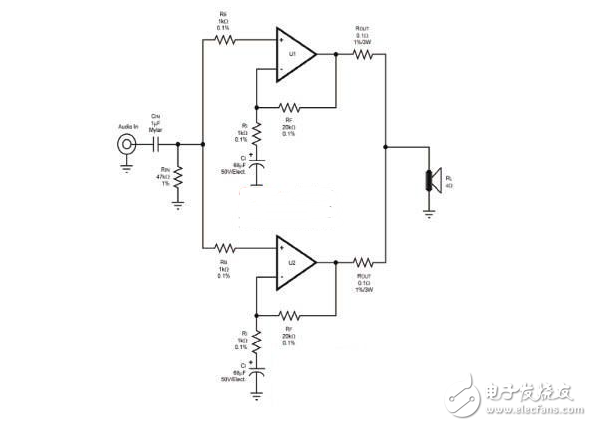
Figure 1 Class AB power amplifier parallel application
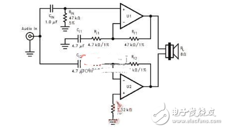
Figure 2 Class AB amplifier LM3886 bridge application
stability
The stability of the design application is important, and the imperfection of the design is likely to cause oscillation. There are many reasons for the oscillation. One of the most common types of oscillations is that the negative half of the waveform has a glitch that produces "(fuzz)". Oscillation does not only occur in the negative half cycle, but every point on the sine wave is likely to occur.
There are three general solutions for oscillating. The first is to add a buffer. Add an RC snubber circuit (also called a zobel phase shifting network) at the output. The second is the amplifier gain method. Most of the AB classes. The power amplifier requires a closed-loop gain greater than 10 times. A feedback capacitor is added to the feedback circuit to increase the stability of the circuit. The third is to improve the power supply and install a high-frequency filter capacitor close to the device.
Heat dissipation factor
All IC products have heat loss, and Class AB power has a large amount of heat generated during operation. The different power consumption depends on the supply voltage and the output load (8Ω or 4Ω).
The heat dissipation depends on the thermal resistance of the IC's own package. Θja refers to “thermal resistance of junction and environmentâ€, and θjc refers to “thermal resistance of junction and outer casingâ€. The heat sink is also a thermal resistance in °C/W, θCS refers to “thermal resistance of the outer casing and the heat sinkâ€, and θSA refers to “thermal resistance of the heat sink and the environmentâ€.
PDMax = V2/(2&TImes;2RLoad)+PQ
Among them, V is the power supply voltage and PQ is the static power consumption.
PDMAX value of LM1875
PDMAX=(50&TImes;50)/(2&TImes;(3.14)2&TImes;8)+(50V×70mA)
PDMAX=15.35+3.5=18.85W
Most IC data sheets have a corresponding “power†curve, which is the easiest way to find the PDMAX value. Not all power consumption under working conditions can be found from the graph. It is necessary to ensure that the horn load corresponds to the selected “power†graph, as shown in Figure 3.
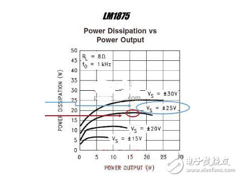
Figure 3 LM1875 power consumption curve
Regarding the calculation of the device temperature, first calculate the total thermal resistance of the chip, assuming that the thermal resistance of the heat sink is 2 ° C / W.
LM1875 (θjc + heat sink thermal resistance) = (3 ° C / W + 2 ° C / W) = 5 ° C / W
Considering that the maximum temperature of the chip does not exceed 150 ° C, if the maximum ambient temperature is 50 ° C, the maximum temperature that the chip can reach can be calculated.
(Total thermal resistance) ×PDMAX+T (maximum ambient temperature)=(5°C/W) ×(18.85W)+50°C=144°C
A simple and easy way to find the heat sink specifications is shown in Figure 4. First, find the corresponding PDMAX value on the vertical axis, then determine the maximum ambient temperature on the horizontal axis, and select the appropriate heat sink thermal resistance. Note here that all the lines intersect at 150 °C, which is the maximum temperature of the IC.
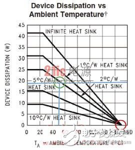
Figure 4 Power consumption and ambient temperature curve
PCB trace
Pay attention to the current between the ground wires when designing the ground wire. From the output signal ground to the power ground, it belongs to a large current ground. The line width of the input signal ground and the output signal ground is already large, but there is still impedance. The current between the ground lines causes the ground line to generate a clutter waveform.
The clutter waveform is generated because the input signal ground is directly connected to the output signal ground. The output signal ground now forms a potential difference from the input signal, and the current flows from the output ground to the input ground. This will add a clutter signal to the input signal of the amplifier.
The ground traces before and after modification are shown in Figure 5. Now the input signal ground and the output signal ground are separately routed, and the two ground lines are connected at a relatively stable ground point (the ground point of the power supply filter capacitor).
High Voltage DC Lithium Battery
High Voltage DC Lithium Battery System
384V High Voltage DC Lithium battery system is manufactured by UFO POWER, designing for telecommunication room, Internet Data Center (IDC), UPS replacement and other core communication areas as an ideal backup power supply. It is equipped with reliable lithium iron phosphate (LiFePO4) battery cell to provide standby power. The lithium battery system consists of 48V LiFePO4 battery modules to form a 384V system in series. The high voltage Lithium battery system uses 19'' Standard Cabinet and the modular design of battery cabinets makes it useful to meet higher energy storage capacities. It can be expanded in parallel according to the need.The High Voltage DC Lithium Battery System is equipped with smart management system. The unit BMU built in the 48V battery module collects battery parameters, including cell voltage, total voltage, charge/discharge current, capacity, temperature, etc.
With centralized monitoring module and LCD Display screen, it allows users to monitor the lithium battery performance in real time, take control of battery and avoid LiFePO4 battery failure.

Features of High Voltage DC Lithium Battery System
â— Safe LiFePO4 Battery Cellsâ— 19'' Standard Cabinet Installation
â— Real-time Monitoring
â— Flexible capacity scalability
â— Wide Application
High Voltage Dc Lithium Battery,High Voltage Lithium Battery,Lithium Ion Battery,High Voltage Lfp Battery
ShenZhen UFO Power Technology Co., Ltd. , https://www.ufobattery.com