Due to the lack of high efficiency of currently used radio frequency power amplifiers (PAs), adding wireless communication capabilities to handheld computing devices requires the use of special power management techniques. Some communication protocols allow for burst transfer techniques that turn off the power supply (with duty cycle control) when no signal is transmitted, but typically do not exceed 40% to 60% of PA efficiency during transmission. Conversely, typical power supply efficiency in handheld devices is typically between 90% and 95%. Many handheld devices work with one to four sections of non-rechargeable alkaline batteries. Other devices associated with backlight displays require the use of higher instantaneous power nickel or even lithium batteries to extend battery life (during charging or battery replacement). Regardless of the type and configuration of the battery, in the modem, in order to ensure a reasonable working life of the system, the modulation and demodulation, PA and RF circuits of the wireless communication require the use of a higher capacity battery.
A typical system, such as a PCMCIA wireless modem, is used to transmit cellular digital data packets (CDPD). Can such a device be plugged into a handheld personal digital assistant (PDA) or run Windows? In a laptop computer of the CE system, a 3.3V power supply consumes only a few hundred milliamps of current. In order to avoid excessive leakage of the main battery, the PCMCIA card usually includes a spare battery. Backup batteries provide power surges during transmission and typically have low equivalent series resistance (ESR), which is common in today's popular rechargeable chemical batteries. The actual power supply of a wireless communication link is primarily dependent on the transmit power and efficiency of the PA.
For example, the power supply (including the backup battery) in the wireless data communication link must interact with the host handheld system operating at 3.3V (Figure 1 - Note the tiny package suitable for handheld systems: IC1 is a 16-pin QSOP package, IC2 Available in an 8-pin μMAX? package). The backup battery is a single-cell lithium-ion battery with a full charge voltage of 4.1V to 4.2V and a residual charge of no less than 2.9V. IC1 converts the backup battery voltage to 3.3V, while IC2 causes the final standby voltage to track the main supply voltage within a 12mV (0.36%) error range.
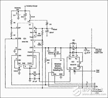
Figure 1. This circuit adds a wireless modem and power amplifier to the handheld device while providing the appropriate power management features.
Tracking the supply voltage is important for the interaction between the wireless hardware and the host. This ensures that the bidirectional data and control lines get the correct logic levels and prevents overcurrent from flowing from the main battery to the modem hardware and from the backup battery to the main battery and electronics.
The circuit works as follows: First, consider the state of the modem before the modem is plugged into the host's PCMCIA slot. Almost no energy or very little energy can be absorbed from the backup battery, so the modem's power supply must be disabled in this state. The switch control line of the standby power supply is the PG pin of IC2. Because the host VHH voltage that powers IC2 does not exist when the modem is not connected, IC2 is in the off state.
When the IC2 power is turned off, the power good (PG) output (internal open-drain n-channel MOSFET) is high impedance, and IC2 only absorbs leakage current. When the PG output is high impedance, two resistor dividers (R6/R7, monitor the backup battery voltage through the IC1 internal comparator, and R3/R4 set the VBOOST level value when the power is turned on) as the pull-up of the ONB line. The resistor turns off the IC1 power supply. Both the IC1 switch mode boost regulator and the low dropout (LDO) regulator are disabled during power-down. Therefore, 1μA leakage current flows into IC1 through a voltage divider and 1mA current, and the battery leakage current is typically 2μA.
Consider the power requirements when powering up: If the power amplifier (PA) must provide 0.6W and 50% efficiency, 1.2W input power is required. If the operation is at 50% duty cycle (the transmission and reception time is equal), then the effective power of the PA is 0.6W. When operating at 3.3V, the load draws approximately 180mA. If the rest of the modem draws 40 mA from the 3.3V supply, the total supply current for the wireless communication link is 220 mA1 when the 3.3V supply is operating.
The IC1 boost regulator provides approximately 800mA at the 2.7V supply input (at the VBOOST pin) and 1A or greater with an intrinsically depleted Li+ battery (2.9V to 3.0V). Even so, the internal low-efficiency LDO is used to power the PA and other modem hardware. The LDO current is nominally 300mA and the minimum rating is 220mA. The main cause is the noise suppression problem. The LDO operates at 300kHz with a PSRR of approximately 38dB, which helps to suppress PWM switching noise on the VBOOST pin. The LDO's built-in filter reduces the need for post-stage noise suppression on the PA supply voltage and associated RF transmit sections or is not required at all, making it easy to pass the Federal Communications Commission (FCC) radiation standards. On the other hand, the intermittent emission efficiency is approximately 8.3%.
VBOOST tracks VHH voltage changes around 3.3V. The backup battery is higher than VBOOST after it is fully charged, and the voltage is lower than VBOOST when the charge is nearly exhausted, so the LDO and boost regulator provide the necessary buck/boost functions in sequence. SEPIC, flyback, and forward configurations are also capable of buck and boost functions, but they all require bulky, expensive electromagnetic storage components (transformers) and lack the noise suppression provided by LDOs. Based on such considerations, the circuit shown in Figure 1 is superior to other solutions.
The next step is to consider what happens when the modem card is plugged into the host's PCMCIA connector. This step is to electrically connect between the corresponding circuit ground (GND) and between all bidirectional data control lines. The host then uses the EN line to enable or disable the modem hardware. If the EN line is initially low during hardware interaction, then all modem hardware will be disabled, presenting a high-impedance characteristic to the LDO node.
Solar Pump Inverter,Solar Pump Control Inverter,Frequency Inverter For Solar Pump,Single Phase Solar Pump Inverter
Zhejiang Kaimin Electric Co., Ltd. , https://www.ckmineinverter.com